This thread has been locked.

If you have a related question, please click the "Ask a related question" button in the top right corner. The newly created question will be automatically linked to this question.

PGA970:please tell me about the SPI response

Part Number: PGA970

Hello, please tell me about the SPI response of PGA970 EVM.
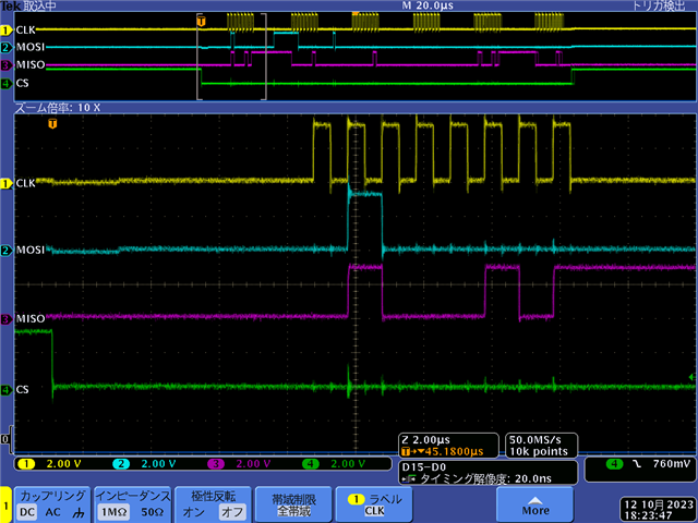
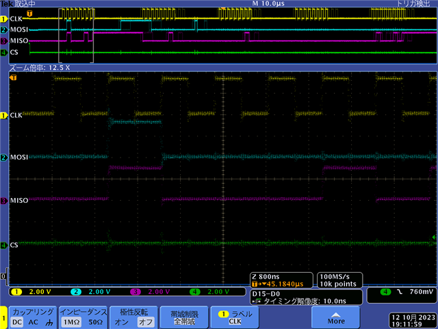
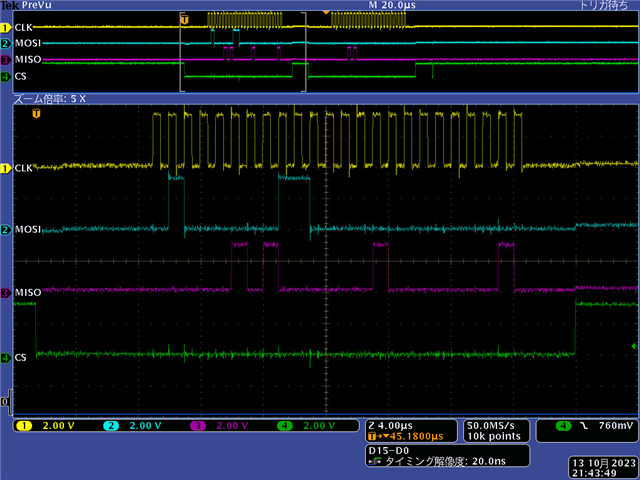
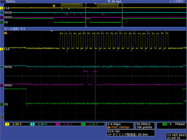
I am trying to read the DIGI_IF_CTRL register (DI PAGE2/OFFSET6) in a test to perform SPI communication with the PGA970.
I sent 6 bytes of 40:C0:00:00:00:00, and the data I received instead was 45:02:02:00:45:02.
The 4th byte was 0x00, not 0x05. The 0x05 response in Figure 34 on page 42 of slds201.pdf is
I couldn't get it.
I checked to see if SPI_EN was set, but when I looked at it with the GUI tool, it was set.

e2e.ti.com/.../pga970-enabling-spi-without-internal-mcu

But it was mentioned as being enabled by default.
How can I get a 0x05 response?

Also, PGA970_Generic_Firmware_Installer.zip contains the SPI function library source file.
I don't think so. Do you have any samples for using SPI?


  • Hi Masae Kawakami,

    Welcome to the E2E forum!  The SPI engine is built into the M0 core and for communication you will have to follow the datasheet information by following the command codes shown in Table 5.  There isn't any additional documentation that you can follow unfortunately.

    I would suggest that you toggle CS between 24 bit transfers.  I would also suggest using the EVM communication and connect a logic analyzer to show you how the communication works.

    Best regards,

    Bob B

  • Hello, thank you for your reply.

    Deassert CS and tdis(CSN) in the time chart of Figure 1 on page 15 of slds201.pdf.
    I tried waiting 4μsec, but I misunderstood the MSB as 8 bits in a byte, so the above oscilloscope wave
    I was waiting in units of bytes. When CS started up in bytes, it got even weirder, so I commented it out.
    It is recommended to write 23 together to prevent misunderstanding of MSB.
    When I deasserted CS in units of 3 bytes and asserted waitCS for 4 μsec, a 0x05 response was returned.
    Thank you. The sent and received data is as follows.
    send 40:c0:00:00:00:00
    recv 05:02:02:05:00:00

    Thanks to your advice I got the 0x05 response.
    The response of the first 3 bytes of the sent command becomes the last 3 bytes of the received data.
    The response of the last 3 bytes of the last sent command becomes the first 3 bytes of the received data.
    The commands sent are DIG_IF_CTRL register read and revision register 1 and 2 read.
    However, if the contents of the DIG_IF_CTRL register (reads 00) are set by power-on default
    OWI_EN and SPI_EN should be 1.
    Are the contents of revision registers 1 and 2 correct at 0x0202?
    The contents of 0-0 and 2-6 when viewed on PGA970GUI were as follows. I still haven't read it...

    When I purchase the PGA970 as an IC, does it include SPI response logic?

  • Hi Masae Kawakami,

    As I said previously, the SPI is a part of the PGA970 base product.  To directly communicate to the PGA970, you need to have the device in a reset state for the microprocessor or if the microprocessor is running you will need to use the COMBUF instead.  When the micro is running and not in a reset state, you cannot access the M0 registers.

    To fully understand the communication flow, I would highly recommend that you connect your scope probes to the SPI interface pins/testpoints and observe the communication when the GUI is operating.  Reading and writing commands to the PGA970 will help you see the communication flow.  I would love to help you more, but I would have to do the same and then show you and explain.  This process is beyond our current support model for these devices.

    https://e2e.ti.com/support/sensors-group/sensors/f/sensors-forum/802433/what-is-the-e2e-support-model-for-the-pga900-and-pga970

    Best regards,

    Bob B