This thread has been locked.

If you have a related question, please click the "Ask a related question" button in the top right corner. The newly created question will be automatically linked to this question.

IWR6843AOP: Custom PCB Boot Issues

Part Number: IWR6843AOP
Other Parts Discussed in Thread: , UNIFLASH

Greetings,

We are developing a product and have an issue with running firmware on a custom pcb with the IWR6843AOP chip.
The hardware is the same as the IWR6843AOPEVM, except it is stripped down of all excess (no bluetooth chip, SOP switches, USB connectors etc).
Only the IWR6843AOP, Crystal (CX2016DB40000D0FLJCC), Spi flash (MX25R1635FZUIH0) and a Power Management IC (LP87524JRNFRQ1) are placed.
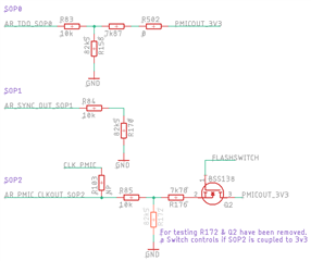
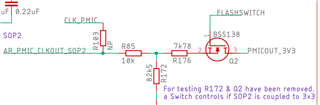
The Power management, decoupling, SOP pins, and other Pull-up's & Down's are copied from the Development kit (IWR6843AOPEVM schematics & Layout).

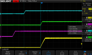
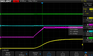
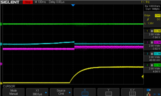
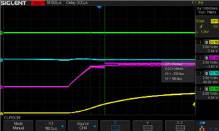
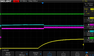
When testing the PCB we followed the hardware implementation excel document (www.ti.com/.../swrr161) and found a problem when checking T3-9
"Measure the voltages on the "1p4V_APLL" and 1p4V_SYNTH" pins". Pin 1.4V_SYNTH does not have 1.4V, if I am correct this pin won't be high until the application is running and RF frontend started. So, why won't that happen?

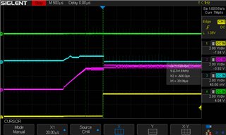
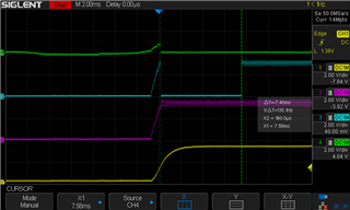
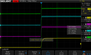
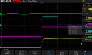
When going further we were able to flash the out of box demo (from IWR6843AOPEVM) with Uniflash (SOP2 set to logic "1", flashing after reset). Programming works the first time the device is powered on. The second time it does not work, but if we turn off the device for a minute it works again.

After succesful flashing SOP2 is set to logic "0" and the power is cycled. If we now sent commands to the flashing UART we receive an echo of the sent command.
The baudrate is 57.6k sending and receiving, other baudrates do not work. I would expect to be talking to the CLI that is implemented in the firmware, but this is not the case.

Some Hardware information:

SOP0 - Pulled to logic "1";
SOP1 - Pulled to logic "0" measures 0V;
SOP2 - Switchable between logic "1" and "0", measured 0V and 1.85V (according to datasheet it needs to be above 1.57v to be registered as logic "1").

Power is OK, the voltages are:
- 1.0V;
- 1.2V;
- 1.8V;
- 3.3V, this VIO voltage does have a slight ripple.

When measuring crystal oscilating frequency we see 40MHz.

JTAG is added to this board, tested quickly but did not work.
We did not document this process, it was quick and we should try this again.

Some findings
- SPI Flash is programmed at 80MHz, I would expect 40MHz.
- In order to boot in functional mode or flash mode the device needs to be powered off for 1 minute.

Kind regards,
Yves

  • Hi Yves,

    1. Yes, it is correct that the voltages on the "1p4V_APLL" and 1p4V_SYNTH" pins will only come up only after RF_init API has been executed, Hence if you power up and check voltage it will still be zero. Hence, we need to check this voltage only when it's chirping. 

    2. The QSPI Flash is programmed at 80MHz. The QSPI clock speed is increased to 80MHz from 40MHz to reduce the boot time for the flash loading.

    3. It suggests that the device is not in correct SOP mode after 2nd NRESET release. We need to check every supply properly, if it's reaching the device. We should probe all the power supply from the source till the IWR6843AOP device and ensure that they are within the datasheet specifications. The nReset signal also needs to be checked. If SOP lines are set to the right state. Sometimes if the power supplies are out of spec limits or correct SOP modes are not latched during nReset the device may not boot up in correct SOP mode. 

    Sometimes the device may boot up during initial power up due to overshoots. Please capture the SOP modes signal after 2nd NRESET release as well as the power supplies. The power supplies and SOP signals should be stable before the NRESET release for device to latch correct bootmode. 

    Regards

    Ankit

  • Thanks for the answers, we got to work and came with some measurements.

    Measuring Power Supply

    Power supply is within spec and all supplies are on, sequence is shown below.

    Blue is 1.0v, Green is 1.2v, Purple is 1.8v, Yellow is 3.3v.

    Measuring SOP’s

    Yellow is nRESET, Purple is SOP0, Blue is SOP1, Green is SOP2

    SOP measurement With 100n on nRESET, as in devkit but without gate (1st nRESET):

    Same setup, 2nd nRESET:

    Not much settling time so we tried a bit more capitance on the nRESET line, shown below.

    SOP measurement with 200n on nRESET (1st nRESET):

    Same setup, 2nd nRESET:

    SOP’s seem to check out but nRESET signal comes on slow. Later we tried to use an STM32g031 to control the reset signal so we could have a controllable signal with less rise time. Results below:

    Made no difference in behavior, same after 2nd reset.

    Measuring warmRESET

    Yellow is nRESET, Purple is SOP0, Blue is warmRESET, Green is SOP2

    As you can see the warmRESET is as expected, no faults here.

    Measuring nERROR_OUT

    Yellow is nRESET, Purple is SOP0, Blue is nERROR_OUT, Green is SOP2

    SOP’s are configured to Flashing Mode:

    As you can see in the above picture there are no errors in Flashing mode, but…

    When the SOP’s are configured to Functional Mode:

    In Functional mode “nERROR_OUT” shows an error, but not in Flashing mode.

    Findings

    NRST_PMIC is HIGH, so device is not in reset

    I2C_SCL & I2C_SDA to PMIC are pulled high, but we do not see data.

  • Hello Yves,

    Thanks for the oscilloscope captures. Also, NERROUT high during functional mode suggests some error in the hardware can we probe through the path of SOP switches to the device and check what is pulling it low during the 2nd reset.  Also please use 200n delay on the NRESET or STM32g031 to avoid incorrect boot mode latching as done in few captures.

    Can you please share the schematic for the SOP settings.

    Regards

    Ankit

  • Hi Ankit,

    Thanks for your response.

    You can find the SOP schematics below:


    Now that I look at it there is no active pulldown on SOP2, just tested it with a pulldown resistor, but no difference in behavior.

  • Yves,

    The schematic seems to be correct. Some signal is pulling the SOP0 low after 2nd reset. Is JTAG connected to the device? Can you check if AR_TDO_SOP0 is pulling down the SOP signal. Or any other signals that could be connected to it (DCA, external host which may have internal pull down).

    Regards

    Ankit

  • Hi Ankit,

    There is nothing else connected to "AR_TDO_SOP0", only what you see in the schematic above.
    In all above measurements there is nothing connected to JTAG (no XDS110 and not even cables).

    Kind regards,
    Yves

  • Hi Yves,

    Please share the complete schematic for review.

    Regards

    Ankit

  • Schematic Custom Board.pdf

    Hello Ankit,

    I have attached the schematic as *.pdf.

    Kind regards,
    Yves

  • Hi Yves,

    Thank you sending the schematic; I have put it in the queue for schematic review and will respond by the end of next week with feedback. Please make sure the device is starting up by probing the XTAL capacitors(40MHz) and VBGAP (0.9V).

    Meanwhile, could you please try connecting JTAG again and read the SOP registers.

    SOP mode register: FFFF E268 (Flash mode should read 0x00000005, Functional Mode should read 0x00000001)

     Regards

    Ankit

  • Hi Yves,

    I checked that R172 and Q2 have been removed, how are you switching the SOP2 to 0 to be in functional mode. Also, please confirm if CLK_PMIC is DNP

    Were you able to connect to JTAG and read the SOP mode register?

    Regards

    Ankit