This thread has been locked.

If you have a related question, please click the "Ask a related question" button in the top right corner. The newly created question will be automatically linked to this question.

IWR6843: Schematic Review

Part Number: IWR6843

Dear TI-

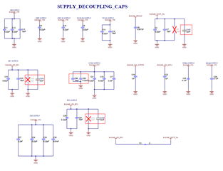
I am attaching my schematic for the IWR6843 radar for your review. My application is long-range people detection. This design uses two identical radar boards to enable a 180-degree field of view.

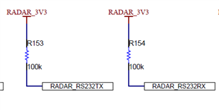
Do I need more I/O signals besides the two UARTs (Command and Log), the SOP2 pin for uploading the code, and the hardware reset? Ideally, I would like to coordinate the two radar boards to avoid interference. This is possible using the sensor start and stop commands. But I was hoping for an indication of when best to start and stop the individual radar (maybe the sync_in signal?) Mine is not a super time-critical application like cruise control, so the simple UART start/stop commands commands may be sufficient. 

I appreciate any feedback/recommendations.

Mike Schell

PS Do I need to add any pull-ups or pull-downs? The spec sheet indicates that most pins have this built into the chip.

IWR6843 Radar Schematics.pdf

  • Hello Mike,

    Thanks for reaching out to us. We have started the schematic review process and shall provide the feedback within a week.

    You will need only two UARTs (Command and Log) if you don't intend to use any other peripherals such as I2C, SPI, LVDS. To synchronize both the radar chips to start frame triggering at the same time you should be using the SYNC_IN signal. Please reach out in case of any further query.

    Regards

    Ankit

  • Hello Mike,

    Please find below the recommendations:

    1. The VOUT_PA, VIN_13RF1, VIN_13RF2 should not be shorted to together. Short only VOUT_PA and VIN_13RF2 through a 0 Ohm resistor only.

    2. Please follow the decoupling capacitors requirements as given below in TI reference schematic.

    3. You will need only two UARTs (Command and Log) if you don't intend to use any other peripherals such as I2C, SPI, LVDS. Please confirm if you will need any other interfaces?

    4. Please add a 220nF capacitor across NRST signal to add RC delay to ensure the reset release is only after the power supplies and SOP signals are stable.

    5. The SOP0 is pulled up and SOP1,2 are pulled low. Please confirm if the device is intended to be used in functional mode only?

    6. To use the BGA ball pin F14 as MSS_UARTB_TX. The pin should be pinmuxed to mode 6 as given below from its default mode of SPI_CLK.

    7. QSPI_D2 BGA pin should be R14.

    8. Please provide pull ups to QSPI_CS (47.5KOhm) QSPI_D2 and D3(10KOhm, 10KOhm respectively)

    9. Please provide weak pull ups of 100KOhm to RS232 lines as shown below. Also, MSS_UARTB_TX.

    10. Please check if the XTAL part follows the datasheet specs as given below:

    Please follow the TI reference schematic given below for more clarity. 

    www.ti.com/.../swrr164

    Regards

    Ankit

  • Hi Ankit-

    Thanks for the very valuable feedback! I failed to explain that the radar board will be connected to the host MCU, which will control a couple of the radar signals, which I will explain in more detail below.

    Comments 1 & 2: Thank you. I have corrected the power supply section to match the reference board, adding a 0-ohm resistor between VOUT_PA and VIN_13RF2. 

    Comment 3: Yes, we only need the two UART interfaces from the radar. I2C, SPI, and other controls will be processed via the external MCU.

    Comment 4: The NRST line is controlled by the external MCU. We will hold the radar in reset until all the power supplies are stabilized.

    Comment 5: The SOP0 line is pulled high, while the SOP1 is held low. The SOP2 line will kept low during regular operation but set high (via the MCU) when we wish to update the QSPI flash. After changing the SOP2 line we will initiate a hardware reset to activate the new mode (flashing or normal).

    Comment 6: We copied this functionality from the reference schematics; Pin F14 is connected to the MSSB_UART_TX. So I assume the pinmux is handled in the driver software already (we use the long-range people detection).

    Comment 7: Thank you, good catch.

    Comments 8 and 9: We added these pullups per your recommendation.

    Comment 10: I double-checked the crystal, which easily meets these specifications. The frequency tolerance is 10 ppm. Thanks for asking.

    Question: We would like to adjust the crystal load capacitors to hit the 40 MHz frequency as close as possible. Does the chip output a clock on any pin that I could measure? It can be the 40 MHz master clock or even a derived clock. 

    Thank you for the feedback and suggestions. I have a couple of software questions, which I will post separately.

    Best-

    Mike

  • Hi Mike,

    The clock output can be measured from the XTALP and XTALM capacitors through the oscilloscope.

    Regards

    Ankit

  • Hi Ankit-

    Thank you. We will find a low capacitance probe so as not to add more load to the caps.

    Best-

    Mike