


Other Parts Discussed in Thread: , UNIFLASH
Hi Support team,
Refer to the circuit of IWR6843AOPEVM to design the homemade PCBA of IWR6843AOP.
The circuit schematic is provided below.
mmWave detection platform_V1.1_20230901.pdf
*Symptom:
The self-made PCBA of IWR6843AOP failed to be burned using uniflash.
The error message is shown below.
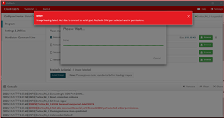
=>I found this error message, which is the same as the situation when IWR6843AOPEVM SOP2 is set to LOW.
*What I checked so far on the hardware side:
- The voltage supply chip(TI LP87524J) delivers 1.2, 1.0, 1.8 and 3.3 as expected.
- VBGAP ~= 0.89V
- RADAR_VOUT_14APLL ~= 1.36V
- RADAR_VOUT_14SYNTH ~= 0V
- An external quartz provides the correct 40 MHz on CLKP and CLKM
- RADAR_OSC_CLKOUT ~= 1.36V
- SOP has been set to FLASH MODE:
SOP2 ~= 2.37V (>1.57 => HI)
SOP1 ~= 0V (<0.65 => LOW)
SOP0 ~= 3.3V (>1.57 => HI)
(3.3V Mode) VIL = 0.65V (MIN) / VIH = 1.57V (MAX)
*Others:
- QSPI FLASH Memory originally used Macronix/MX25R1635FZUIL0, which has been changed to TI BOM SET: Macronix/MX25R1635FZUIH0.
I would like to ask in which direction can I conduct hardware measurement and confirmation?
If possible, please help me review the circuit schematic diagram. Thank you.

