Hello,
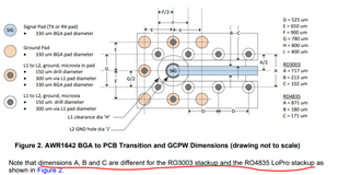
1. Can you please provide information about the landing pattern (BGA to PCB transition) for the TX/RX bumps of IWR6243? Is it the same for RO3003 and RO4835 stackup as outlined in Figure 2 of the "TI mmWave Radar sensor RF PCB Design, Manufacturing and Validation Guide" ?
2. Ideally, we would like to use a different stackup. How can we obtain the HFSS models (package + die ?) that can help us in our impedance matching design?
Thanks!