This thread has been locked.

If you have a related question, please click the "Ask a related question" button in the top right corner. The newly created question will be automatically linked to this question.

AWR2944: DCC Dual Clock Comparator Configuration

Part Number: AWR2944

In the AWR2944 Datasheet it states: 

Device architecture supports Four Digital Clock Comparators (EDCCs) and an internal
RCOSC. Dual functionality is provided by these modules – Clock detection and Clock
Monitoring.
EDCCA is dedicated for ADPLL/APLL lock detection monitoring, comparing the ADPLL/
APLL output divided version with the Reference input clock of the device. Failure detection
for EDCCA could be programmed to cause the device to go into limp mode.
Additionally, there is a provision to feed an external reference clock to monitor the internal
clock using the EDCCA.
EDCCB, EDCCC, EDCCD module is one which is available for user software. From the
list of clock options given in detailed spec, any two clocks can be compared. One example
usage is to compare the CPU clock with the Reference or internal RCOSC clock source.
Failure detection is indicated to the MSS R5F CPU via Error Signaling Module (ESM).

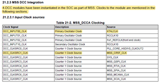
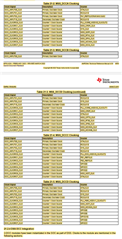
However in the TRM it shows the Clocks that can be compared for MSS_DCAA, MSS_DCAB, MSS_DCCC and MSS_DCCD as shown below: 
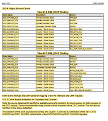
Also two for DSS_DCAA and DSS_DCCB as shown: 
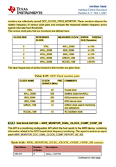
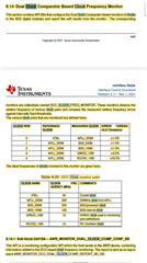
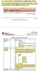
The mmWave Radar document section 8.14, DCC_CLOCK_FREQ_MONITOR (see below) shows various clock pairs clock pairs which look at the frequency and measure the errors.  It gives the Reference clock and the measured clock and the error threshold for each.  It also gives the clock name and frequency for each.  Through the API 0x01DC- AWR_MONITOR_DUAL_CLOCK_COMP_CONF_SB the different clock pairs can be enabled by setting bits b0, b1, b2, b3 or b4 to 1.  The comparison results are in the monitoring report message.  

Questions:

1. Why does the datasheet say DCAA is reserved and the TRM give options for clock comparision?

2. Why does the mmWave document define clock comparisons in section 8.14 for DCC pairs if they are also shown in the TRM as having various other input clock sources?

3. Section 21.2.2 Clock Source Selection for Counter0 and Counter1 states to reference the datasheet to identify the available options for selection the clock sources for both counters of the DCC module.  The datasheet states "From the list of clock options given in detailed spec, any two clocks can be compared. One example usage is to compare the CPU clock with the Reference or internal RCOSC clock
source." However, the mmWave document gives clock pairs that can be turned on and off and reported. 

        3a) Which is document is correct and how are the pairs chosen? 

        3b) Are the ones in the mmWave document defaults and are they ready to enable (may required register configurations of course)?  

        3c) It appears that the documents are not clear and the TRM is for multiple products where the datasheet and mmWave may be more specific for the AWR2944, is that true?  
  • Hello George,

    Can you please share the revision number of the documents you are referring to?

    Thanks

    Regards,

    Ajay

  • AWR294x_TRM_SPUIV5A_V8 Technical Reference Manual v0.8, AWR2944 Datasheet SWRS273 - NOVEMBER 2021 and mmWave Radar Interface Control Document Revision 3.17.   

  • Still looking for a response to my above questions is someone can provide clarification: 

    Questions:

    1. Why does the datasheet say DCAA is reserved and the TRM give options for clock comparison?

    2. Why does the mmWave document define clock comparisons in section 8.14 for DCC pairs if they are also shown in the TRM as having various other input clock sources?

    3. Section 21.2.2 Clock Source Selection for Counter0 and Counter1 states to reference the datasheet to identify the available options for selection the clock sources for both counters of the DCC module.  The datasheet states "From the list of clock options given in detailed spec, any two clocks can be compared. One example usage is to compare the CPU clock with the Reference or internal RCOSC clock
    source." However, the mmWave document gives clock pairs that can be turned on and off and reported. 

            3a) Which is document is correct and how are the pairs chosen? 

            3b) Are the ones in the mmWave document defaults and are they ready to enable (may required register configurations of course)?  

            3c) It appears that the documents are not clear and the TRM is for multiple products where the datasheet and mmWave may be more specific for the AWR2944, is that true? 
  • Hi George,

    Please find my comments below.

    1. Why does the datasheet say DCAA is reserved and the TRM give options for clock comparison?

    The TRM provides the complete configuration available for the device. As per the safety manual we recommend using DCCA for PLL lock detection of the APLL and hence the datasheet lists the fact that the DCCA should be reserved by the user and used to check the APLL clock output. Since clock is a major factor for functional safety, the user should reserve this for the above-mentioned mechanism. 

    2. Why does the mmWave document define clock comparisons in section 8.14 for DCC pairs if they are also shown in the TRM as having various other input clock sources?

    AWR2944 has 3 sub systems. The MSS, DSS and RSS. The MSS has 4 instances of the DCC module, DSS has 2 instances, and one instance is in RSS. The RSS one is not mentioned in the TRM or datasheet as it is configured and used by the TI firmware to add safety mechanisms for the RSS.

    The mmwave link document refers to the module present in the RSS only. The TRM provides details about the MSS and DSS instances only. 

    Hence the difference that you observe. Both documents refer to different instances of the DCC module present in different sub systems. 

      3a) Which is document is correct and how are the pairs chosen? 

    This is explained in Q2 response above. 

    3b) Are the ones in the mmWave document defaults and are they ready to enable (may required register configurations of course)?  

    This is explained in Q2 response above. 

      3c) It appears that the documents are not clear and the TRM is for multiple products where the datasheet and mmWave may be more specific for the AWR2944, is that true? 

    TRM is specific to AWR294x devices. 

    Thanks,

    Pradipta.

  • Please confirm: So from the mmWave for the RSS system it shows that XTAL compared to the APLL which is actually chosen in the MSS system and described in the TRM.  The rest of the clock pairs for the RSS system are then compared to the APLL_200M with the error thresholds given and enabled in Sub block 0x01DA - AWR_Monitor_DUAL_CLOCK_COMP_CONF_SB?    The other 3 MSS clocks are then still open for SW use?     

  • Hi,

    Please find my comments below. 

    Please confirm: So from the mmWave for the RSS system it shows that XTAL compared to the APLL which is actually chosen in the MSS system and described in the TRM.

    No, APLL is not chosen in the MSS system. The options for DCCA in MSS is XTAL for reference and MSS_CR5_CLK which is 300 MHz. In RSS the clock that is provided as input to the subsystem (APLL_200M) is checked. Every sub system is checking its specific input clock. 

    Please check the clock tree block diagram for more clarity on this. 

    The other 3 MSS clocks are then still open for SW use?   

    Yes, they are open to use, and suggestions are also provided in the safety manual of the device on what can be checked using the rest of the DCC instances.

    Thanks,

    Pradipta. 

  • The RSS is showing that the XTAL is the reference clock and the measured clock is then APLL_200M, From your comments above for the TRM the MSS shows primary oscillator clock is XTALCLK and Counter 1 Clock Source is MSS_CR5F_CLK which is 300MHz.   

    Thank you.