This thread has been locked.

If you have a related question, please click the "Ask a related question" button in the top right corner. The newly created question will be automatically linked to this question.

OPT3001EVM:Technical question EVM design

Part Number: OPT3001EVM
Other Parts Discussed in Thread: OPT3101

Hi ti Team

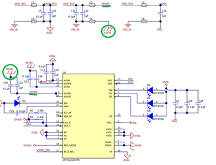
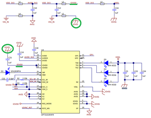
There is a difference in the ground reference for the capacitors on pins 9 and 10 of the OPT3101 IOVDD line.

In the EVM design the capacitors are referenced to the ground of the VDD_LED line

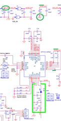
In one of the reference designs they are referenced to the IOVDD digital ground

I have two questions about how to reference these capacitors to ground.

What is the correct line to reference those capacitors to ground?

Are these capacitors necessary? Can we connect directly to the IOVDD_DUT line without placing the capacitors C29 and C30 First image?

  • Guillermo,

      All of the grounds are technically at the same level and also connected together. What we know is that VDDL and VSSL provides the current path for the emitters. There will be high currents and high frequencies.(173mA at 10Mhz) Attempts to isolate the current noise from the rest of the circuit was made by adding ferrite beads to power and ground. These small boards make it hard to isolate the current path to only the one part of the circuit. Personally I don't like ferrite bead on the ground of any circuit, however they do prove to help keep the emitter currents out of the other power supply paths. Select ferrite beads with low resistance and high impedance. (<0.1Ohm DC resistance and >400Ohms at 100Mhz)

    Idealy the different currents in the circuit would have a seperate path and the grounds would connect at the input ground of the PCB. Then ferrite beads would only be uesd on the AVDD, IOVDD and the VDDL rails. If you can accomplish this task you will be better off in your layout. 

    Keep the power and ground planes or traces as low of an impedance and resistance as possible, and seperate the current paths. I would use RF layout techniques for this board. You will be fine keeping to these guide lines.  

    For reference see https://www.ti.com/lit/ml/slyp173/slyp173.pdf?ts=1701278322263&ref_url=https%253A%252F%252Fwww.google.com%252F - High Speed PCB Layout Techniques