Hi team,
I have a customer who will post a couple questions on E2E regarding this part - it's been handled by the industrial radar team but given the level of support requested, we've decided to move this to E2E for the automotive team to handle. Let me know if you'd like me to send you the threads we've handled over email thus far. I'll put one of the questions below, and Matthew Berberich should follow up on his end of things in a separate thread. See below for the request from Bernard.
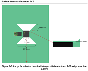
"We are currently looking into the layout requirements we have to adhere to in order to mitigate the surface wave artifact mentioned in the errata document SWRZ115A and discussed in the email threads below. Recall, this describes a requirement to keep the PCB board edge close to the Antenna on Package (AoP) device in the E-plane to minimize the surface waves that cause ripple in the antenna gain response. It also suggests that if the board is large and the IC is centralized then cutouts need to be made in order to break the surface wave as shown below:
"
I would like a little further clarification and direction on the mitigation requirements
- One clarification I would like to know with the notched approach is if this is primarily concerned with the conductive planes in the PCB supporting the surface wave or if the notch actually needs to be completely free of any material including dielectric?
- Related to this also, would placing a metal or dielectric structure behind the PCB (like a plastic or metal housing) pose any problem with the antenna performance? Is there a distance requirement for such objects residing beneath the notched areas and the PCB in general?
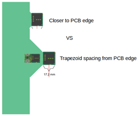
- Below I also sketch the possible arrangement of placing the IC on only one end of the PCB. In this case would one need to maintain the trapezoidal cutout along the ground edge or could the part be place closer to the main board without being detrimental to the antenna performance?"

Thanks in advance
Marco

