Other Parts Discussed in Thread: AWR1843AOP
Hello,
I have a question about AWR1843AOPEVM PCB.
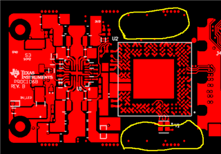
Regarding Layer1 pattern of EVM PCB, please let me know why the GND pattern is removed around AWR1843AOP.

Plese advise.
Best regards,
Shoko
This thread has been locked.
If you have a related question, please click the "Ask a related question" button in the top right corner. The newly created question will be automatically linked to this question.
Hello,
I have a question about AWR1843AOPEVM PCB.
Regarding Layer1 pattern of EVM PCB, please let me know why the GND pattern is removed around AWR1843AOP.

Plese advise.
Best regards,
Shoko
Hello Shoko-san,
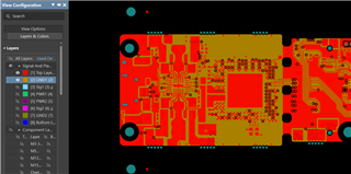
There should still be ground - e.g. see below:

Hello James,
I have alredy know there is GND pattern on Layer2.
I want to know why there is not GND pattern around AWR1843AOP on LAYER1.
If you don't know about it, could you please change to someone who can be expert on PCB pattern?
Please advise.
Best regards,
Shoko
Hello Shoko-san,
I'm following up with my team about this. However, may I ask why you want to know about this? Here are my thoughts:
1. for antenna performance, the ground in the next layer down is sufficient for ground, and the design was simulated thusly. Additionally, since this is AOP its important to not have any 'incorrect' structures too close to the antenna that could impact the antenna's performance/pattern/matching etc.
Regards,
James
Hello Shoko-san,
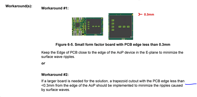
After checking with my team, I understand that this was done to eliminate surface wave effects near the antenna. Generally speaking, we do suggest there to be no PCB above and below the device (even though this is not 100% followed in the reference design, that is the general recommendation).
AWR1843AOP Device Errata, Silicon Revision 1.0 (Rev. A) (ti.com)

Regards,
James