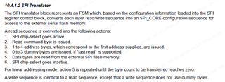
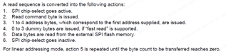
This thread has been locked.

If you have a related question, please click the "Ask a related question" button in the top right corner. The newly created question will be automatically linked to this question.

AWR2944: Improve QSPI with DMA enable read speed

Part Number: AWR2944

Hello Expert,

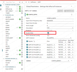
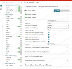
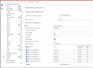
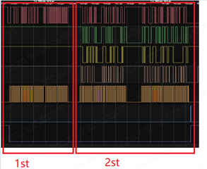
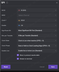
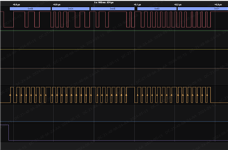
We set the QSPI input frequency to 80MHz and enabled DMA. Then, I observed the following clock signal waveform(read flash).
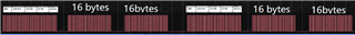
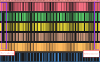
CMD Address   Data Data CMD Address   Data Data
6BH A23-A16 A15-A8 A7-A0 dummy 16bytes data 16bytes data 6BH A23-A16 A15-A8 A7-A0 dummy 16bytes data 16bytes data

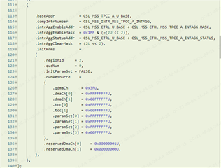
For every 32 bytes read, a command/address/dummy must be sent. Which is differenct with the discriptions of AWR294x Technical Reference Manual(action 5 is repeated until the byte count to be transferred reaches zero)

Is it correct? What does cause it? How to change our configuration to repeat action 5 until the byte count is zero?

Regards,

Wu Bin

  • Hello Wu bin,

    Could you let me know what software are you using? Along with the version as well?
    And are you reading the address linearly here?
    Based on this I will need to cross check with my team on the internal behavior.

    Regards,
    Saswat Kumar

  • Hello Saswat Kumar

    Based on the "sbl_qspi" demo from the SDK(mcu_plus_sdk_awr294x_09_00_00_15), 

    1. Enabe DMA for QSPI configuration.

    2. Add CONFIG_EDMA1 for EDMA_MSS_A configuration and the conguration parameters of CONFIG_EDMA1 is default value.

    3. flash configuration links to CONFIG_EDMA1

    Regards,
    Wu Bin

  • Yes, the address is linear and continuous.

  • Hello Wu bin,

    Have you done any modifications on the SBL, by default it should be doing the QSPI read in memmap mode.

    Regards,
    Saswat Kumar 

  • Hello Saswat Kumar

    We didn't modify the QSPI mode which is still memmap mode. The description is also from SFI Translator.

    We only enabled EDMA which configure QSPI as EDMA memmap mode.

    If we have not made any modifications to the SBL, the sequence for read is (CMD + ADDR + DUMMY + 1BYTE + CMD + ADDR + DUMMY + 1BYTE ...) instead of (CMD + ADDR + DUMMY + 1BYTE + 1BYTE  + 1BYTE ...)

    Regards,

    Wu Bin

  • Hello Wu bin,

    So without the EDMA you are seeing the right sequence in the read from QSPI?

    Regards,
    Saswat Kumar

  • Hello Saswat Kumar,

    No. Such as, I want to read 1024 bytes. The expected sequence from the descriptions below is CMD + ADDR + DUMMY + 1024 bytes DATA.

    However the actual sequence is 1st(CMD + ADDR + DUMMY + 1 byte data)  + 2st(CMD + ADDR + DUMMY + 1 byte data) ... + 1024st(CMD + ADDR + DUMMY + 1 byte data))

    Regards,


    Wu Bin

  • Hello wu bin,

    Sorry for delay as there was holiday in india.

    The team wants the entire log of the logic analyzer if possible, can you please send that so that we can analyze? This log should contain the entire logic analyzer from start to end of the SBL boot.

    Regards,

    Saswat Kumar

  • Hello Saswat Kumar,

    It seems that I cannot share the logic log file with you directly, so I will seek to share it with you through the FAE in the China region.

    We will share two files:

    sdk_04_06_00_01_QSPI_with_DMA.sal : EDMA is enabled for QSPI

    sdk_04_06_00_01_QSPI_without_DMA.sal : EDMA is disabled for QSPI

    The each file contains two segments:

    1st is TI rom boot for loading SBL with 40MHZ QSPI frequency 

    2st is SBL with 80MHZ QSPI frequency 

    Regards,

    Wu Bin

  • Hello Saswat Kumar,

    The attached is the log of the logic analyzer.

    logic_log.rar

    Regards,

    Wu Bin

  • Hello Wu bin,

    Also can you tell me how are you identifying the whether it is a CMD or address from the logs. I don't think QSPI is an extension by default in logic analyzer and its becoming a little hard for us to identify.
    IS there some method you are following to identify easily which is the command and which is the address and data, etc.

    Regards,
    Saswat Kumar

  • Hello Saswat Kumar,

    The data I've captured with my logic analyzer isn't quite accurate; we can only make a rough analysis.

    The new data in the attached is relatively better quality. Hope it is useful for you. 

    7713.logic_log.rar

    In the first part of the diagram below, only SI (IO0) has data, so this section is CMD(1bytes) + ADDR(3bytes)+ dummy(1bytes).

    in the second part, IO0~IO3 have data all, so this section is data segment.

    Regards,

    Wu Bin

  • Hello Saswat Kumar,

    It's also possible to roughly view the data for command plus address via SPI configuration.

    Regards,

    Wu Bin

  • Hello Wu bin,

    Thanks a lot for this, will provide some feedback on this by friday after analyzing.
    in case any other concerns I will let you know in this thread.

    Regards,
    Saswat Kumar

  • Hello Wu bin,

    When I am analyzing your logs:

    That is not exactly just 16 - 16 bytes right? It is a lot more bytes, so I am confused ow you are saying that between 2 commands there are 16-16 bytes each.

    We are only considering the command valid when the io1 , io2 and io3 all are high outputs(high impedance) and only when the command on line io0 is 6B
    So we see a lot of data getting transferred from your plot.

    Regards,
    Saswat Kumar