Other Parts Discussed in Thread: IWR1443
Tool/software:
I am trying to simulate the Antenna in Ansys HFSS present in the module the results are not matching. I need assistance to solve this problem.
This thread has been locked.
If you have a related question, please click the "Ask a related question" button in the top right corner. The newly created question will be automatically linked to this question.
Tool/software:
I am trying to simulate the Antenna in Ansys HFSS present in the module the results are not matching. I need assistance to solve this problem.
Hello,
Can you please share the results you are referring to here.
Thanks,
E. Shareef
Dear Satish,
This is funny. I am just working in the same area. I have tried to import the Altium data from sprr253.zip available on
https://www.ti.com/tool/IWR1443BOOST#technicaldocuments
but have enormously problems to import correct data to Ansys. So far I got a layer stack with all the unneeded vias and routes. My antenna field simulations are nonsense. If you still need some help, pls call back again. Maybe within the next days I have a solution for my project and can tell you.
BR Bernd
You will need to export ODB files from Altium, then use Andy's Simulink to generate .aedt file for HFSS simulations.
But we can provide HFSS files directly for the antenna simulations on 2944 if needed. I believe that is what Satish is referring to here.
Thanks,
E. Shareef
This would be the easiest way. In my situation I have no access to Altium and Simulink produced a lot of layers I could not delete. So I converted the PCB to Ansys after reading the ODB from spr253.zip. To whom it may concern, I have prepared a recipe:
<-----> Start
open Ansys Electronic Desktop (I am using 2024R1.1)
in project manager delete "project1"
File -> Import -> ODB++...
navigate to: "...\sprr253\Altium_IWR1443_revB_DesignSchematicLayout\PROC010 Web Deliverables\PROC010 Web Deliverables\PROC010B_Gerbers\PROC010B_Gerbers\ODB"
you see the file "PROC010B.tgz", select it and open
the ODB++ Import menue opens
leave all layers selected
leave all nets selected
press "ok" button
* wait for import
now you see the full design
zoom in in the area of antennas with mouse wheel
you see, copper is not filled, there is only the ladder
move mouse outside the sketch and press right mouse button
open view display mode and select solid
* all copper traces are filled
click on layers dialog
set "Disply" to "All Layers"
deselect all layers with marker in frist column and in second column -> user header
select "top, Dielectric_1, l2" in first and second column
press "Apply" and check to see only these 3 layers
click again on layers dialog (activation of layers)
deselect "l2, Dielectric_1"
apply and close
now, you see top layer
remove all parts and rout you don't want to see included in EM simulation
-> find IWR1443 in layout, at 7 o'clock there is a quartz
assume in mind a vertical line left to the quartz
delete all components and routes left to this vertical line
*
activate layer "l2" and "Dielectric_1"
for drawing select "l2" from list menue
drwa a rect on l2 with the size, you wish
select "Dielectric_1" from list menue
draw a rect with the same size of l2
* don't forget to save your work
activate top layer
set orientaion to right
rotate the board (maybe use fit all)
you might change the color of the dielectricum
* save
view top
fit all
mark the boxes on bottom of layout and delete
* save
edit the layer stack
check file on TI e2e "">e2e.ti.com/.../iwr1443-dielectric-constant-discrepancy-for-rogers-4835-on-iwr1443boost-reference-design
set the DK for the correct layer
* save
in layerstack editor check all layers, uncheck the desired 3 we need
make all visible, except our 3 important
"apply and close"
fit all
delete all figures
open layerstack menue
remove each layer, except out first 3
* apply and close, view if okay and save
now, place ports on pins of IWR1443, I started left bottom and placed anticlockwise
*
you might do a Geometry Check, I made it three times with healing
* save
define analysis single and sweep
* save and "Analyze"
Validate -> no errors / all green checked
* calculating frequency points (6 at the same time): RAM 132 GB in use
>>>>>>
at this point, I selected all structures in drawing and use the function "Unite"
this connected all overlapping and touching figures together
*
check if ports are on vias "top" to "top"
*
try simulation, wait ... wait ... wait, I was waiting for half a day
* create reports and check S-parameters
* create gain plot
>
>
> good luck
<-----> End

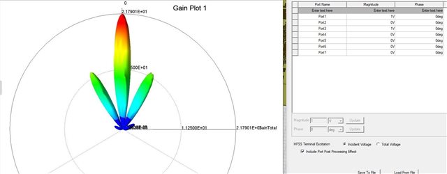
... let me summarize: The antenna patterns are really good! Congratulations to TI and the engineers they prepared the patterns. After one has the layout ready for analysis, it is also possible to analyse the patterns only. Just remove all parts of layout up to the reference plane where the little step is in the antenna feeding line.
I am really impressed! The figure above shows a feeding at TX1 and TX3 with mag 1 and 0 degree. All other ports are not feeded.