This thread has been locked.

If you have a related question, please click the "Ask a related question" button in the top right corner. The newly created question will be automatically linked to this question.

IWRL6432AOP: Schematic Check Request for L6432AOP side

Part Number: IWRL6432AOP

Tool/software:

Hi L6432AOP Champ !

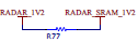
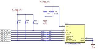
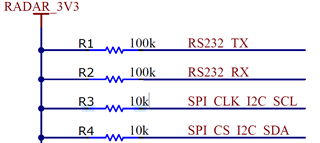
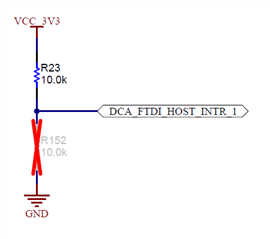
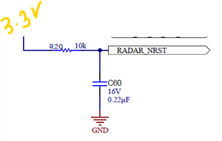
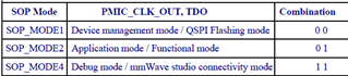
Can you please check the custom circuit design especially for bootmode, power rail, memory, connector which could be based on IWRL6432AOP? 

My customer has done for Sensor area firstly, and used connector (8CON5) to connect to expandable area.

kspl2405_f_device_radar_6432_ws_rev01_20240724.pdf

Thanks, and Regards, 

Jack 

  • Hi Jack,

    Could you please create a jira request for the same.

    https://jira.itg.ti.com/browse/HARDWARE_APPS

    Regards

    Ankit

  • Hi Ankit

    Is it allowed for external customer to access the site above? I'm unable to access it for now.

    Regards, Jack

  • Hi Ankit.

    Please check S25FL064LVF01 interface. 

    Thanks.

  • Hi Jack,

    I have added it to schematic review queue.

    Regards

    Ankit

  • Hi Jack,

    We completed the schematic review and found various major errors. I would recommend the customer to follow the IWRL6432AOP EVM design below.

    https://www.ti.com/lit/zip/sprr496

    1. RADAR_SRAM_OUT is not connected to 1.2V power supply. For 3 rail power optimized SRAM_OUT should be connected to RADAR_1V2 and RADAR_1P2_RF.

    2. Currently LDO is being used for supply 1.2V and 1.8V which is not recommended kindly use the DC regulator with the below criteria or follow TI reference design.

    Meets peak current requirement per rail 
    Low quiescent current, High efficiency
    Forced PWM or PFM/PWM mode control
    Spread spectrum clocking
    PGOOD Feature
    Small package size
    Higher Switching Frequency (3.5MHz - 4MHz)

    3. The QSPI Flash does not have QE bit enable by default. Also, the pull up for QSPI_D3 and QSPI_CS are incorrect.  QSPI_D3 should have 10KOhm pull up and QSPI_CS should have 47.5KOhm pull up not vice versa. Also, kindly use the Flash with the below criteria.

    Clock frequency greater than or equal to 80MHz
    Quad Enable (QE) bit is 1
    Fast read, program and erase time
    The Flash memory should be equal or lesser than 64Mbit
    Low power consumption
    Supports SFDP command
    Smaller package size

    4. Kindly check the voltage divider R6550 and R6651 value for correct output of 3.3V

    5. Essential pull ups and pull down are missing for interfaces and critical signals.

    6. NRESET RC delay circuit is missing.

    6. VPP is connected, are they using an authenticated boot device? VPP should be DNP for GP devices.

    7. SOP0 and SOP1 are undefined. SOP0 and SOP1 should be defined for correct boot up.

    8. XTAL external load capacitance should be 4.7pF and not 15pF

    9. Please check the correct decoupling capacitor from TI EVM reference design.