Tool/software:
Hello,
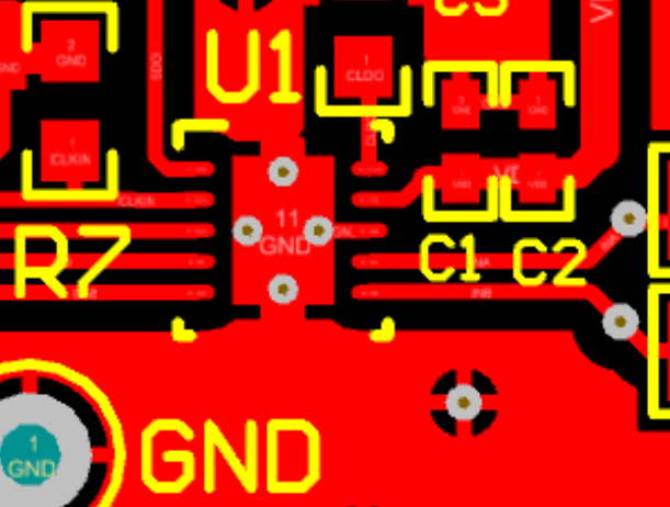
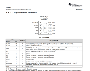
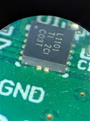
The pinout sketched in the datasheet doesn't illustrate the ground pins on the ends of the LDC1101 package. I could not find a clear layout guideline for this part.
The ground pins on the sides are seen in the EVM layout soldermask layer

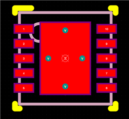
I found this attached USON guideline on these TI forums and it seems to match. Can you confirm this attachment is 0410.DRC10_ePOD_4218878_datasheet.pdfTI's recommendation for the LDC1101 PCB footprint?


 .
.