This thread has been locked.

If you have a related question, please click the "Ask a related question" button in the top right corner. The newly created question will be automatically linked to this question.

TMP126: TMP126

Part Number: TMP126
Other Parts Discussed in Thread: , INA229

Tool/software:

Hi,

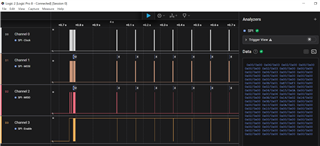
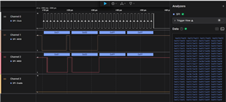
I am using an STM32F469BIT7 microcontroller to communicate with the TMP126 chip via the SPI1 bus. However, I am encountering an issue where the chip does not respond to commands such as reading the Config Register, Temp Result Register, THIGH_Limit, and TLOW_Limit register values.

As per my understanding, the TMP126 requires 16-bit data transfers. Therefore, I have configured my SPI bus to communicate using a 16-bit data frame.

According to the TMP126 datasheet, "Data is clocked out on the falling edge of the serial clock (SCLK), while data is clocked in on the rising edge of SCLK." This suggests that the SPI mode should be 1, where CPOL = 0 and CPHA = 1.

Here are the SPI settings I have configured:

  • SPI Speed: 5.625 MHz
  • CPOL: 0
  • CPHA: 1
  • Data Size: 16 bits

The SPI bus is configured as follows:

// Set the SPI parameters
Spi1Handle_power_board.Instance               = SPI1_POWER_BOARD;
Spi1Handle_power_board.Init.BaudRatePrescaler = SPI_BAUDRATEPRESCALER_32;
Spi1Handle_power_board.Init.Direction         = SPI_DIRECTION_2LINES;
Spi1Handle_power_board.Init.CLKPhase          = SPI_PHASE_2EDGE;
Spi1Handle_power_board.Init.CLKPolarity       = SPI_POLARITY_LOW;
Spi1Handle_power_board.Init.DataSize          = SPI_DATASIZE_16BIT;
Spi1Handle_power_board.Init.FirstBit          = SPI_FIRSTBIT_MSB;
Spi1Handle_power_board.Init.TIMode            = SPI_TIMODE_DISABLE;
Spi1Handle_power_board.Init.CRCCalculation    = SPI_CRCCALCULATION_DISABLE;
Spi1Handle_power_board.Init.CRCPolynomial     = SEVEN;
Spi1Handle_power_board.Init.NSS               = SPI_NSS_SOFT;
Spi1Handle_power_board.Init.Mode              = SPI_MODE_MASTER;
Please find the schematic attached for your reference. Could you please advise what I might be doing wrong? Thank you for your help!
  • I believe it should be CPOL=0 and CPHA=0. Typically, a mistake here would result in bit-shifted data instead of no-data. However, TMP126 may be ignoring a command word it does not understand. 

    I'm also concerned that you may struggle to achieve 5MHz with the 10kohm resistor. Have you looked at the communication with an oscilloscope?

    thanks,

    ren

  • I have been monitoring the transactions using a Logic Analyzer. When CPHA is set to 1, no data is shifted. However, when CPHA is set to 0, data is shifted.

    According to the datasheet, the TMP126 can operate at a maximum of 10 MHz. I initially configured it to 5.625 MHz but later changed it to 0.7 MHz as you recommended and captured the data for your reference. Despite this, I still encounter issues with chip configuration and data reading.

    Below is a snapshot when CPHA = 1:

    Data representation (Micro DataOut / Micro DataIn):

    1. First Data: Write command for configuration register (reset command): RegAddr = 0x0003, Data = 0x0100
    2. Delay: 1 ms
    3. Second Data: Write command for configuration register: RegAddr = 0x0003, Data = 0x0002 (Continuous Conversion 62.5 ms)
    4. Third Data: Read command to verify the configuration register. Responds with 0x0000

    The rest follows the configuration for the Alert Enable register, Temp Low Limit, High Limit, Hysteresis, Temperature Slew Rate Limit, and continuous temperature result register.

    When CPHA = 1, the write command values are proper, but there is no response from the TMP126.

    The below snapshot is to show the synchronization between the data and SCLK.

    Below is a snapshot when CPHA = 0:

    It appears that the write/read command values are disturbed while sending them over the SPI bus, as shown below:

    The below snapshot is to show the synchronization between the data and SCLK.

  • Hi Ren,

    I have tested all four SPI modes (combinations of CPOL and CPHA), and Mode 1 is the only one that outputs the correct value on the SPI bus. I also tried varying the frequency as follows:

    • 90 MHz / 256 = 350 kHz
    • 90 MHz / 128 = 700 kHz
    • 90 MHz / 64 = 1.4 MHz
    • 90 MHz / 32 = 2.8125 MHz
    • 90 MHz / 16 = 5.625 MHz

    However, there is no response or zero response from the TMP126. I am unsure what else to try to get it working. Your assistance would be greatly appreciated!

  • You will have to configure both your host controller and your logic analyzer for the same CPOL and CPHA settings to avoid having the data appear shifted or incorrect in the analyzer. 

    Looking at the TMP126EVM, I can see that it is using CPOL=1 CPHA=1 communication as shown here:

    The data shown is the shared SIO pin at the TMP126. I'm not able to probe the MOSI pin before the resistor like in your setup. Note that the host must transmit 0xFF 0xFF for the 3rd and 4th bytes to allow the TMP126 to respond during this period. I don't see this happening in your captures.

    I recommended using CPOL=0 CPHA=0 because the datasheet shows the clock idling low. I can change the TMP126EVM GUI to transmit using CPOL=0 CPHA=0 and it looks like this:

    Both of the transactions I'm sharing are a read of the device ID register 0x0C. My prototype TMP126 is reporting an ID of 0x0126 where the datasheet states a production sample should report 0x2126. At any rate, CPOL1/CPHA1 is a complementary configuration to CPOL0/CPHA0. As you can see, they both work with TMP126. However, a CPOL1/CPHA0 or CPOL0/CPHA1 configuration will be incompatible with TMP126. 

    Let me know if this helps clear up your confusion regarding CPOL/CPHA. 

    I did notice that something is pulling down your MISO line during the first byte. This shouldn't be coming from TMP126 - are your SPI pins shared with another device?

    Your analyzer is capable of logging analog, and I would like to see it if you could share it. This is to address the pull-up and bus frequency concern.

    thanks,

    ren

  • Agreed! I have set my Logic Analyzer to CPOL = 0 and CPHA = 0.

    The GPIO pins are configured as part of the SPI setup, with the pins set to No Pull/Down. I don't believe the pins should be configured with a Pull-Up. It shouldn't matter because the same SPI configuration works perfectly with multiple INA229 chips, regardless of whether the SPI GPIO pins are set to PULLDOWN, NOPULL, or PULLUP. Just for your information.

    However, I have changed the configuration to Pull-Up on the GPIO pins, and I observe that the pins are high during the idle state. The chip is responding, but the values are not correct.

    Most of the time, the data received is identical to the data sent.


    Additionally, SPI1 is shared among 3 TMP126 sensors and 2 INA229 chips.

  • Pull-up implies the pin is limiting its drive strength. Can you configure your MOSI pin for its full drive strength? The 10kohm resistor is limiting the MOSI's ability to control MISO/SIO, so it should not be further handicapped by its configuration. Your MISO should be an input-only with no pull. You are still showing strange behavior on your MISO that suggests the pin is not stable. You should be looking at this in analog. It will likely show you that the level is moving around, as if floating.

    thanks,

    ren

  • I am a bit confused. The recommendations you have been providing so far are not mentioned anywhere in the datasheet.

    For example:

    • The dummy bytes should be 0xFF, not 0x00.
    • What will be the frequency proportional to the variable resistor value on the MOSI pin?
    • I don't see any information regarding the drive capability of the MOSI pin based on the variable resistor value.

    My recommendation is to include all this information in the datasheet to make it easier for us to implement correctly.

    Could you please confirm if the following configuration is what you are recommending? This is what I have been following:

    On the microcontroller end:

    • SCLK: No pull
    • MISO: No pull
    • MOSI: No pull

    For your information, I am able to read the temperature values when I configure the prescaler to 256.

    90 MHz / 256 = 350 kHz

  • Hi Ren,

    Thank you so much for your support!

    I am able to figure it out and make it work except it is not clear how low the resistor value can go to achieve higher frequencies and the chip drive that MOSI pin correctly!

  • The resistor on MOSI is used to make MOSI perform like an open-drain driver. It does this by limiting current sourced from MOSI. If you are configuring the GPIO to also limit its drive strength, it will be even weaker than intended. 

    The TMP126 has a single bidirectional SIO pin for data transfer. Sometimes SIO will be an output, and sometimes it will be an input. We can't connect the SIO, which will sometimes act as an output, directly to another output, MOSI. If one of the two outputs attempts to sink current for a logic low while the other output attempts to source current for a logic high, there will be a large current flow that only stops when one of them breaks. To prevent this, we've put a resistor on MOSI to limit its output current. This makes its behavior similar to a bus with open-drain outputs: the rise time of the signal is now limited by the RC circuit formed by the resistor and any parasitic capacitance. If you could disable your MOSI output before the TMP126 SIO becomes an output, you could avoid this problem without using the resistor. You would have to carefully control this in software to avoid causing damage to the hardware. If you did this, you would avoid the RC circuit and the poor rise time, enabling potentially higher clock rates. This is why I've advised you to enable analog capture of your SIO pin and observe the rise/fall times. Your resistor and parasitic capacitance may not support the maximum clock rate of the TMP126.

    thanks,

    ren