This thread has been locked.

If you have a related question, please click the "Ask a related question" button in the top right corner. The newly created question will be automatically linked to this question.

TUSS4470: Signal to noise ratio - Unused driving circuit - EMI

Part Number: TUSS4470

Tool/software:

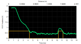
1. The datasheet for the TUSS4470 indicates that the output peak to peak noise varies from 75mV to 300mV with a 5V supply.

     What would be the typical peak to peak noise? Does it apply to all the dynamic range or does it vary along the dynamic range?

     Does the "Receiver path dynamic range" specification take into account the peak to peak noise?

2. The block diagram seems to indicate that the output driver circuit is independent of the analog receiver.

     Is there any specific constraint to be aware of if the transducer is driven by an external circuit and only the analog receiver is used?

3. EMI susceptibility is a concern.

    It looks like the receive input circuit uses a differential stage. With the calculations providing different component values for Cinp and Cinn,

    does it increase EMI susceptibility? What would be the requirements of Cinp, Cinn, Rinp for best EMI susceptibility immunity?

    Was there any test done on EMI susceptibility for the device? If so what are the results?

  • Hello,

    Thanks for posting to the sensors forum! Let me help address your questions:

    1. Output peak-to peak noise

    • What would be the typical peak to peak noise?
      • Not specified since the typical noise can vary.
    • Does it apply to all the dynamic range or does it vary along the dynamic range?
      • Specification applies to the entire dynamic range but only under the configurations shared in the datasheet
    • Does the "Receiver path dynamic range" specification take into account the peak to peak noise?
      • The receiver dynamic range is not influenced by the output peak to peak noise. But the ability to show the entire dynamic range is affected by the peak to peak noise hence why this is not taken into consideration for this spec.

    2. Output driver and receiver

    •      Is there any specific constraint to be aware of if the transducer is driven by an external circuit and only the analog receiver is used?
      • The stages are separated, but there is none as long as there is good frequency matching between all transducers to ensure signals are received properly.

    3. EMI susceptibility.

    • It looks like the receive input circuit uses a differential stage, does it increase EMI susceptibility?
      • I am not sure, but it may depend on what EMI standard/test you are considering. Do you mind sharing what EMI susceptibility test is of concern here?
    • What would be the requirements of Cinp, Cinn, Rinp for best EMI susceptibility immunity?
      • This may vary on the test as well as pass fail requirements. Please share any information that may be necessary.
    • Was there any test done on EMI susceptibility for the device?
      • No tests have been performed to my knowledge

    Best,

    Isaac

  • 1. The datasheet specifies that the typical "Minimum receive input" is 2.4uV (-26.4dBv) and the "Maximum receive input" is 48mV (-112.4dBv). Thus a difference of 86dB which is within the range of the "Receiver path dynamic range (minimum to maximum output)" of 82dB to 92dB.

    The graph of Figure 6-2 indicates that for a 40 or 256 KHz signal the 2.4uV starts at around an output of 0.5V (more or less the pedestal) and ends at around 3.8V. Since this seems to indicate that the "Receiver path dynamic range (minimum to maximum output)" is above the pedestal, what does the "Receiver path dynamic Range(noise floor to maximum input)" represents if it doesn't take into account the output peak to peak noise?

    2.  Are pins VPWR, VDRV, OUTA, OUTB, GND left not connected or grounded to ensure proper functionality, minimal noise and EMI susceptibility?

    3. The EMI specifications of concern is:

    • Radiated Susceptibility / Immunity.
    • Frequency Range: 5 MHz to 5 GHz.
    • Field Strength: 50 Volts/Meter
    • Waveforms: (a) Continuous Wave, (b) 80% Amplitude Modulation at 1kHz, and (c) Pulsed.
    • Standard: ISO 11452-2.
  • Typo correction in 1: 2.4uV(-112.4dBv), 48mV(-26.4dBv)

  • Hello Mike,

    Sorry for the delay.

    1. For the DR_AFE spec on the receiver path it does take into consideration the peak to peak noise along with the output pedestal level, sorry for the confusion on this one. 
    2. OUTA, OUTB, VDRV, VPWR, IO1 and IO2 can be connected to ground if they will not be used.
    3. Thanks for the details, this is definitely a test we have not looked into performing for this device, typically we get ISO standard requests from customers for parts in our automotive portfolio, the TUSS4470 is part of our industrial portfolio so we have not looked into performing this test. I wish I had more insight as to what you could do that would help you pass this standard with this device but I dont have much insight to provide here. If you do run tests please let me know if there are any questions/issues that I can help out here.

    Best,

    Isaac

  • Hello Isaac,

    I don't consider that there was a delay in the response.

    Thanks,

  • Hello Isaac,

    I have a doubt and would like confirmation. In the datasheet I looks like VPWR powers the driver circuit only, which is why I added it to the list of pins to ground or not if the driver circuit is not used, assuming that the receiver circuit is powered by VDD. Can you confirm that VDD effectively powers the receiver circuit as I will be using it.

    Thanks,

  • Hello Mike,

    I am fairly certain that is the case but this should be fairly easy for me to test out. I can try this out in the lab and get back to you, I should have some time to look into it tomorrow and I can get back to you then.

    Best,

    Isaac

  • Hello Isaac,

    That's fine. I need to be sure so I don't need a respin of the board because of an assumption.

    As a side note, we have talked with a contact in the digital group if it still possible to talk with an FAE, specifically on this device, and the recommendation is to go through this process. I'm creating a design with the TUSS 44x0 to replace an existing design with another chip with the goal of getting prototypes for the end of the year. Thus I probably will have other questions. I am not sure if you are the person that would be answering them.

    I had one on the shape of the output and from the description in the datasheet the receive signal went through a pre-amp, a filter, the logamp then the output buffer. There was no mention of detectors in the logamp stages or other method to recuperate the RSSI (envelop of the signal) which seems to indicate that the output is basically the amplified oscillations of the received signal. However I found in one of the post that you mentioned the output is the envelop.

    Another related question is on the filter which seems to be between the output of the logamp and the output buffer and the associated external capacitor on the FLT pin. I'm trying to understand what does that filter actually do. Is it just a low pass filter? What does the FLT capacitor actually do?

    Also the equation on Vout is confusing, specifically within the log section. The units don't add up. Glna and Gbpf have no units, Vin is in volts, INTlog is in dBv and Kx has no units. So you end up with Volts/dB for which you take the log. My guess was to convert the INTlog in volts to get the units to line up, however the results don't match the curve. What am I missing?

    The purpose of these questions is to understand what will affect the shape of the Vout curve and how, based on the type of signal received.

    Thanks,

  • Hello Isaac,

    Additional questions on Cinn and Cinp. Our design will have an active filter in front of the input of the TUSS44x0 with transducers operating between 100KHz and 200KHz. There is a series resistor at the output of the last opamp to adapt impedance and provide maximum signal.

    I find that the recommended Cinp value results in a fairly high impedance in that frequency range. Given the active filter and output resistor as described, what would be the optimum Cinp and output resistor values?

    Is there any disadvantage to increase the value of Cinn beyond the calculated value? Is there any limit (e.g 1uF)?

    Thanks,

  • Hello Mike,

    Typically FAEs will forward questions unless if they are highly familiar with the products, so its still likely that questions would still go directly to me. You can still get in touch with your analog FAE if you have one assigned to you since they can always help you with other questions you may have.

    Do you mind sharing which device you are replacing so that I can have a better understanding of the differences?

    Regarding your question on the envelope of the signal, the TUSS4470 does not provide the amplified oscillations on the output but it does provide the envelope of the signal. Output example captured over ADC:

    • I'm trying to understand what does that filter actually do. Is it just a low pass filter?
      • Correct this is just a low pass filter
    • What does the FLT capacitor actually do?
      • The flt capacitor is used to configure the cutoff frequency of the filter.
    • Also the equation on Vout is confusing, specifically within the log section. The units don't add up. What am I missing?
      • I have looked into this before. If I recall correctly there was definitely something missing. I need to look through my notes for this.
    • I find that the recommended Cinp value results in a fairly high impedance in that frequency range. Given the active filter and output resistor as described, what would be the optimum Cinp and output resistor values?
      • The main purpose of the C_INP and R_INP components are to protect the input stage of the TUSS44x0, its pretty common to connect this pin directly to your driving stage when using a monostatic topology so we need to protect this pin somehow, I know this is not the case for your application since you dont plan on even driving a transducer. It's still recommended when separating it from the drive stage but you can definitely reduce the impedance here if necessary. C_INP is needed to AC couple and limit the current going in the pin while R_INP is mainly used for additional current limiting. Keep in mind the current limit at I_INP is 15mA.
    • Is there any disadvantage to increase the value of Cinn beyond the calculated value? Is there any limit (e.g 1uF)?
      • C_INN capacitor is used to help limit current on the I_INP line and is part of the filter network of the analog front end, so increasing beyond the calculated value may begin to filter out some of the necessary signal.

    I still need to check on the VPWR question. I should be able to have a confirmation on that item today.

    Best,

    Isaac

  • Hi Isaac,

    Thanks for these answers and your time on it.

    Filter capacitor

    If I were to guess, in the Cflt equation of Table 8-1 6250 is Rlpf (from datasheet) and 25 is the factor chosen to minimize the attenuation at the transducer frequency. The fact that the equation is linked to the transducer frequency suggests that the extraction of the envelop is done through this filter and not via detectors within the logamp stages. Thus I can't just view the filter as a filter for the resulting envelop after extraction. Is this correct?

    Cinp, Cinn

    Thanks for clarifying this. I had assumed that Cinp and Cinn were only used to ensure there were no DC component interfering with the input stage. So I'll use the value from the equation for Cinn. I'll need a little bit more for Cinp. The circuit before Cinp will basically consist of the ouput of an opamp with a resistor in series followed by decoupling capacitors for high frequency components (noise & EMI mitigation), then the Cinp capacitor. Limiting the current could be done with the series resistor only and use a high value for Cinp ensuring a consistent transfer (tolerance on resistor 1%, tolerance on capacitor 10%), however I might transfer just a fraction of the signal. So to optimize the series resistor and Cinp values I would at least need the input impedance of the TUSS44x0.

    Device being replaced

    I just received the authorization from my customer on this. The device is the SA614. It's principally an FM chip and only the RSSI function was used. I can ask if I can share more details but even so I would prefer this information to be outside the post.

  • Hello Mike,

    • Filter capacitor
      • I believe there are detectors in the logamp stage this might just not be information we publicize on the datasheet. I would need to look through some of our design documentation to confirm that this is in fact the case and that the filter is not used for the envelope extraction.
    • Cinp, Cinn
      • I can get you this info, it might take some time since I would need design info for this. They are mostly out of office this week for the holiday.
    • Device being replaced
      • I dont think I need any additional detail, I just wanted to confirm the part but we have had a handful of customers switch from the SA614 to the TUSS44x0 family since the EOL of the SA device. So I feel fairly confident saying that you are looking at the right device and that the TUSS44x0 should most likely be able to accomplish what you are trying to do in your design.

    Best,

    Isaac

  • Hello Isaac,

    Filter capacitor

    That makes sense. The filter is probably fed the detectors output where it has to filter out the 2x input frequency of the demodulated signal. What I am trying to figure out is how much I can use the value of the filter capacitor to control noise at the expense of rising and falling time of the envelop signal, without affecting the logamp slope, which appears to be the case for the TUSS44x0.

    Cinp, Cinn

    Next week is fine if you can manage it. The components indicated will be in the design so layout can proceed without the correct values.

    VPWR

    Were you able to test and confirm if Vdd powers the receiver section?

    Thanks,

  • Hello Mike,

    • Filter capacitor
      • I read through some of the design documentation and there are detectors in the log amp stage that provide the full wave rectification but you are correct the LPF filter stage created with the FLT capacitor is used to extract the envelope of the signal. But this will definitely affect your rising and falling time of the envelope signal.
    • Cinp, Cinn
      • Yeah I think I should be able to get some details on this next week for you to make a better calculation using the impedance of the input.
    • VPWR
      • Yes, I was able to confirm that VPWR is not necessary in order for the digital blocks to run. You would only require the Vdd.

    Best,

    Isaac

  • Hello Isaac,

    Great! Appreciate your answers. I'll wait on the Cinp,Cinn question and if you can find what's wrong with the Vout equation.

    Thanks,

  • Hello Isaac,

    I went through the various registers and have a few questions.

    DEV_CTRL_1: LOGAMP_SLOPE_ADJ

    The equations are missing some explanations. I assumed for VOUT_SCALE_SEL  that if the parameter was set for 3.3V in the equations you use 5V for VOUT_SCALE_SEL with a bar on top and 3.3V with no bar. For VOUT_SCALE_SEL at 3.3V this results for LOGAMP_SLOPE_ADJ from 0 to 7 in 30.048, 31.043, 32.038, 33.033, 26.002, 27.030, 28.025, and 29.020. I checked the numbers against the slope of Figure 6-13 and it matches. It's also in line with the non adjusted slope SLafe of 29.7 (Section 6.7). If these results are correct, it implies the units are wrong at the end of the equations. The slope is linear when the input voltage is expressed in dB so the units are mV/dB which is what is also used to specify the non adjusted slope SLafe.

    The problem is that it doesn't work if VOUT_SCALE_SEL is 5V. The results are around 32mV/dB whereas they should be around 45mV/dB. Am I making the wrong assumption in the equations?

    ECHO_INT_CONFIG: ECHO_INT_THR_SEL

    I assumed that in this case the equation uses the ECHO_INT_THR_SEL value (0 to 15) which results in thresholds from 400mV to 1000mV for 3.3V and 600mV to 1500mV for 5V.  It seems strange that it doesn't cover a wider range. Is this correct?

    ZC_CONFIG: ZC_CMP_IN_SEL

    I understand the use of INP and INN to detect zero crossing of the signal, however there is no description of VCM that I could find anywhere else in the datasheet. What is VCM?

    ZC_CONFIG: ZC_CMP_STG_SEL

    I assume the stage refer the the logamp stages. How many stages does the logamp has and for which stage does the parameter values from 0 to 3 correspond?

    Thanks,

  • Hi Mike,

    Isaac is currently out of office. He should be able to take a look at your question by the end of this week.

    Thank you for your patience.

    Best,
    ~Alicia 

  • Hey Mike, 

    Sorry for the delay on this as I was out of office for the holiday in the US.

    DEV_CTRL_1: LOGAMP_SLOPE_ADJ, Equation 1 for V_OUT

    • There are some items in the formula that missing some info so let me help clarify those
    • G_VOUT: this value should be 1 for 3.3V and 1.5 for 5V
    • SL_LOG: Slope based based on VOUT_SCALE_SEL 29.7mV/dB for 3.3V or 45.1mV/dB for 5V
    • G_LNA: based on setting of the LNA
    • G_BPF: 0.9V/V
    • Vin: Input
    • INT_LOG: value needs to be converted into volts instead of dBV based on reference voltage
      • 20log(Vx/1V), for example using -100dBV, Vx = 10^(-100/20) so Vx= 0.00001V
    • Kx: log amp intercept

    This should line up with the figure you see in the datasheet.

    ECHO_INT_CONFIG: ECHO_INT_THR_SEL

    • Your calculations are correct this is what we spec in the datasheet. 

    ZC_CONFIG: ZC_CMP_IN_SEL

    • I am not certain but it could potentially be a reference voltage internal to the device. I will need to get back to you on this one.

    ZC_CONFIG: ZC_CMP_STG_SEL

    • The log amp contains 7 stages, I will need to check with design to verify which stages correspond to the ZC_CMP_IN_SEL bits.

    Items that are still missing: 

    • Impedance of the input, for CINN and CINP calculations
    • What is the VCM voltage used for ZC comparator
    • What stages are used for the ZC_CMP_IN_SEL 

    Best,

    Isaac

  • Hi Isaac,

    No worry. Hope you enjoyed your holiday.

    DEV_CTRL_1: LOGAMP_SLOPE_ADJ

    I believe the info you provided here answers the question I had on the Vout equation in section 7.3.4 of the datasheet. My thanks for clarifying that equation.

    The question I had for the LOGAMP_SLOPE_ADJ is for the equation in section 7.6.1.3 for that parameter. As I indicated previously I made some assumptions on the VOUT_SCALE_SEL variable in the equation (bar and no bar on top). The results seem to match the curves of Figure  6-13 and the spec of 29.7 mV/dB in section 6.7 for 3.3V. However the equation with the same assumptions doesn't match the curve of Figure 6-2 and the spec of 45 mV/dB for 5.0V.

    ECHO_INT_CONFIG: ECHO_INT_THR_SEL

    Sorry for that one. I was working my way through the registers description and wanted to make sure my assumptions were correct for the ECHO_INT_THR_SEL in the equation. I didn't think to look if there was a spec related to this parameter.

    If possible could you look first for the input impedance. The board layout is completed and we are ordering the PCB. The components will be ordered within the next couple of days.

    Thanks,

  • Hello Mike,

    Here is the information

    DEV_CTRL_1: LOGAMP_SLOPE_ADJ

    I am glad that I was able to get your questions answered on the Vout portion.

    ECHO_INT_CONFIG: ECHO_INT_THR_SEL

    No worries, its always good to check. 

    Here are the answers to the last items we were covering:

    For the input impedance: It is expected to be ~100ohms

    The VCM voltage used for the ZC comparator is an internally generated 0.9V reference.

    The stages used for the ZC comparator are the last 4 stages in the log amp.

    Best,

    Isaac

  • Hello Isaac,

    Thanks for all the research to get those answers. The input impedance value came in just in time. Much appreciated.

    I'm still puzzled about the LOGAMP_SLOPE_ADJ parameter equation and maybe I'm missing something in your answers. This parameter adjust the logamp slope with 7 values (0x0 to 0x7) with each value having a different equation as described in Table 7-9. As I mentioned, if for a supply of 3.3V I set VOUT_SCALE_SEL bar at 5V and VOUT_SCALE_SEL no bar at 3.3V in each equation the resulting slope for each equation looks correct based on what can be derived from the curves of Figure 6-13 and the spec of 29.7mV/dB. However for a supply of 5V, if logically I set VOUT_SCALE_SEL bar at 3.3V and VOUT_SCALE_SEL no bar at 5V, the resulting slope for each equation is not even in the range of 45mV/dB. What are the VOUT_SCALE_SEL bar and VOUT_SCALE_SEL no bar values to use in those equations?

    Thanks,

  • Hello Mike,

    No worries always trying to help out.

    DEV_CTRL_1: LOGAMP_SLOPE_ADJ

    Got it, I think I had missed your question on this and thought it was tied to the Vout calculation. The values that should be used in the LOGAMP_SLOPE_ADJ equation for VOUT_SCALE_SEL should be 0 and 1.

    So when trying to get a 3.3V scale out of your TUSS4470 device the formula would be the following:

    0x0-  (3.0 x 1) + (4.56 x 0)

    When configuring to the 5V scale then the formula would be the following.

    0x0- (3.0 x 0) + (4.56 x 1)

    Best,

    Isaac

  • Hi Isaac,

    In that case, shouldn't the equation read more like as follows since the slope is typically 29.7mV/dB for 3.3V and 45.1mV/dB when the factory slope settings is not overridden. I think the decimal point is at the wrong place.

    0x0- (30 x 1) + (45.6 x 0) for 3.3V

    0x0- (30 x 0) + (45.6 x 1) for 5.0V

    Thanks,

  • Hey Mike,

    Sorry I missed that detail, but that seems like it could be very likely.

    It seems to track fairly well for both configurations and the spec on the datasheet is specifically for 58kHz so it would explain why we are not seeing the full entire range in the min/max. I can reach out to the team and confirm if this is the case, although it may take some time since a lot of the team is starting to take time off for the holidays.

    Best,

    Isaac

  • Hi Isaac,

    I found it odd that the SLafe min/max spec varied that much for a given setting (factory trim), with the max value for 5V an outlier, as I was expecting around 2 mV/dB device to device variation. However it might be meant to indicate the variation depending on the LOGAMP_SLOPE_ADJ value if the factory trim is overridden. In such a possibility the 3V min would be 26mV/dB and max 33mV/dB, and the 5V min would be 39.4mV/dB and max 50.1mV/dB according to the LOGAM_SLOPE_ADJ equations with 10x values.

    I'll assume for now that the LOGAMP_SLOPE_ADJ are as suspected and will wait for your confirmation, and maybe at the same time also check on the meaning of the min/max of the SLafe spec. In the interim, you provided much information that will be used in starting the prototypes which should arrive this week and I can wait for that last bit.

    Enjoy the holidays!

  • Hi Mike,

    Isaac is currently out of office for the holidays and will not be back until the end of the year. When he gets back, he should be able to provide an update on what he's learned. 

    Thank you so much for your patience and happy holidays!

    Best,

    ~Alicia