A related question is a question created from another question. When the related question is created, it will be automatically linked to the original question.
If you have a related question, please click the "Ask a related question" button in the top right corner. The newly created question will be automatically linked to this question.
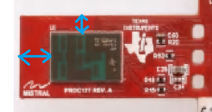
North and South side of the PCB should be as close as possible to the device to reduce the surface wave effects. East and West side of the PCB should have a minimum spacing of one lambda (~5mm) from the device to PCB edge or any other components.