This thread has been locked.

If you have a related question, please click the "Ask a related question" button in the top right corner. The newly created question will be automatically linked to this question.

AWR1843AOP: Hot pad issue

Part Number: AWR1843AOP

Tool/software:

Dears,

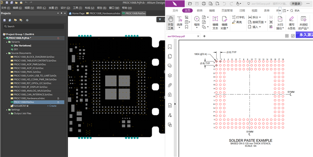
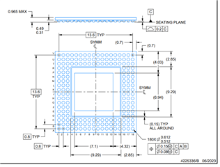
1.1843AOP BGA package, does the reference package in the specification book not have this hot solder pad in the middle? The device itself is not tinned in the middle;
2. In the reference design, there is a hot solder pad and the steel mesh paste layer is also windowed.
Is this one in the middle used for heat dissipation? Is the chip center not tinned? Do you need steel mesh windows?
3. The center of the chip protrudes and is not tinned. It is uncertain whether the steel mesh should be opened, and there is no clear indication from the chip specification sheet. I don't know if opening or not has any impact.

  • Hello,

    Referring to page 84 of the datasheet as shown below, the square in the middle of the package is the exposed die, but the die does not make any contact with the PCB. This area on the PCB is used to improve the thermal dissipation through solder mask opening which can be seen underneath the die in your image above. Using plated thermal vias, the ground connection is made while having a top layer ground copper to improve thermal performance. My suggestion would be to follow the TI reference design. You could also refer to the following app note regarding the thermal design guideline. Thermal Design Guide for Antenna on Package mmWave Sensor

    Regards,

    Aydin