This thread has been locked.

If you have a related question, please click the "Ask a related question" button in the top right corner. The newly created question will be automatically linked to this question.

TMP423: DXP and DXN Waveforms

Part Number: TMP423
Other Parts Discussed in Thread: DXP

Tool/software:

Hi Teams,

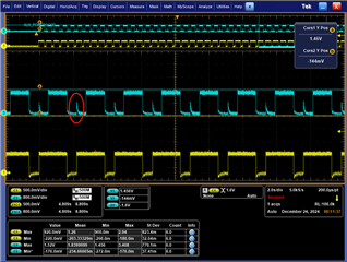
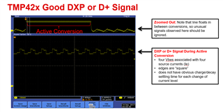
I’d like to confirm some questions regarding the signals on the DXP and DXN pins when VDD = 3.3V with PNP transistors:

  1. As shown in the waveform below, the signals represent DXP and DXN with respect to VSS. For CH2, does the waveform anomaly circled in red affect the test results?
  2. Regarding question 1, based on your experience, could this anomaly be caused by the layout? (If yes, what are your suggestions for improvement?)
  3. At an ambient temperature of 25°C, what voltage levels for DXP and DXN at High are considered reasonable? If we need to refer to the transistor specifications, which parameters would be the most appropriate reference?

  • Hi Sky,

    This scope shot looks a bit unusual, I would expect the voltage on DXP and DXN to track each other. 

    Could you please share the schematic? As well as the measurement configuration? 

    Best,

    Sakeenah

  • Hi Sakeenah 

    The circuit section can refer to the diagram below.
    Previously, the oscilloscope captured DXP3 and DXN.

  • Hi Sky,

    Thanks for sharing the schematic! I will consult my team and try to get back to you on Monday. 

    Sakeenah

  • Hi Sky,

    Here is an example of a good DXP signal. If you zoom in on DXP, you should see 4 different voltage levels within the DXP signal during the active conversion. DXN should be about 0-0.7V. The voltage on DXP depends on the transistor, source current (Ie), and temperature. 

    It looks like there is some noise in your scope shot. Since remote sensors measure very small voltages using very small currents, noise at the device inputs may introduce measurement error. Potential sources of error caused by layout include EMI or inductive coupling and cable/trace resistance. To reduce the noise, you can follow these recommendations: 

    • Shielding of PCB traces
    • Using a shielded cable
    • Routing between layers
    • Trace spacing > 10mils
    • Shorter traces

    What temperature error are you seeing in your measurements? 

    Sakeenah