This thread has been locked.

If you have a related question, please click the "Ask a related question" button in the top right corner. The newly created question will be automatically linked to this question.

AWR6843AOP: HW check list - Resources and FAQ (About antenna)

Part Number: AWR6843AOP

Tool/software:

Hi team,

This is Lina covering Radar in Korea.

My customer asked me some questions about the antenna on the HW check list. 

https://www.ti.com/lit/zip/swrr197 

In that document, There is request for a 20 degree clearance interval from left to right of the IC.

  1. Should the criteria of 20 degrees be based on the IC Package edge?

  2.  If you look at the AOP Data Sheet, the beam angle is 120 degrees x 120 degrees
    I'm curious about the reason why you guide the clearance angle to 20 degrees. If I adjust it to 40 degrees, will there be a significant difference in antenna performance?
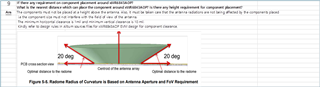
      

Regards,

Lina Kim

  • Hey Lina,

    Thanks for reaching out regarding your questions on hardware bring-up. One of our hardware experts will reach back out to you within the next day or two.

    Regards,

    Kristien

  • Hi Lina,

    Snapshot mentioning 20 degree is taken from the Radome design guide-mmWave Radar Radome Design Guide - where it is simulated for the 140 degree azimuth Field of View (FoV). FoV of AWR6843AoP in azimuth direction is 120 degree. Hence you should consider a clearance angle of 30 degree (on both the sides) from the IC package edge. In Elevation direction PCB edge width should be less than <0.3mm to minimize ripples in radiation pattern. Please refer "Surface Wave Artifact from PCB" Errata - AWR6843AOP Device Errata, Silicon Revision 2.0 (Rev. B). I would recommend to follow EVM layout files for the clearance.

    Thanks and Regards,
    Sivaprasad

  • Hello Sivaprasad,

    Thanks for your help!  Customer gave me additional questions, Could you check it?

    1. PCB Design Guide

      When they checked the 'AWR6843AOP Device Silicon Errata' document you answered, the following is indicated.


      AOP Package is currently placed at 45x30mm PCB Center because it was not possible to check that document during the initial design.

      Q1) Is it necessary to cut the PCB around AOP Package like the document?
      Q2) Or do I just need to not place the top layer copper/parts of the PCB?
      Q3) If they don't cut the PCB and you don't see the large ripple on Simulation, is it okay not to follow the guide?


  • 2. FOV Judgment Criteria


    *WR6843AOP FOV performance is 120 degrees X 120 degrees.
    However, if you look at the FOV measurement DATA of DATA SHEET, it seems that Elevation does not come out at 120 degrees.
    Q1) Could let me know how many dB TI uses for FOV judgment?

    Q2) According to the measurement results below, it seems to be less than 120 degrees even based on 12 dBfs. What are the criteria for TI to say FoV 120x120?

    Q3) Is the result of the measurement when Radome is not present?

  • Hi Lina,
    1) Yes it is strongly recommended to follow the guidelines.
    2)Not placing component near to the elevation direction will not help in this case.
    3) We leave that to customer. We have no problem if they are okay to manage ripple levels on their simulation results.

    I have few more comments on my previous reply. As I mentioned at least 30 degree clearance is needed from FoV perspective. Moreover, it is recommended to place the electromagnetically conductive materials > lambda(wavelength) distance away from IC package edge to eliminate surface wave effects. You can see in the checklist some of the decaps should be placed very close to the BGA ball. In that case decaps can be placed at the bottom near to the BGA ball.

    Thanks and Regards,
    Sivaprasad

  • Hi Lina,
        On an average it is approximately taken 12dBfs to determine FoV. There may be some relaxation slightly.


    Thanks and Regards,
    Sivaprasad

  • Hello Sivaprasad,
    Thanks for your support. I have an additional question.

    Cutting the PCB physically is not easy.
    Instead of physically cutting out the PCB, would it be okay to remove the copper from all layers in the specific area?

    Thanks.

    Best Regards, 
    Beomseok.

  • Hi Beomseok,
    It is necessary to remove complete material on elevation side of the IC as recommended. Just by removing copper from all layers will not help in this case. It is not catastrophic if you didn't make a cutout in the PCB. But according to your end use case please ensure you have enough margin to tolerate these ripples.

    Thanks and Regards,
    Sivaprasad