This thread has been locked.

If you have a related question, please click the "Ask a related question" button in the top right corner. The newly created question will be automatically linked to this question.

HDC2080: Temperture effected by Li-Ion Charging Circuit

Part Number: HDC2080

Tool/software:

Hi

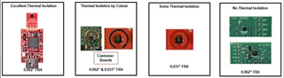
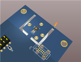
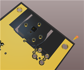
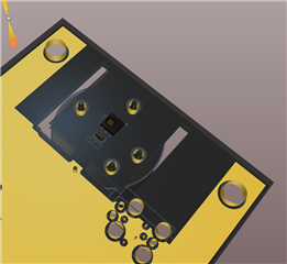
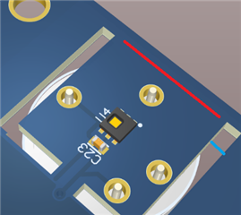
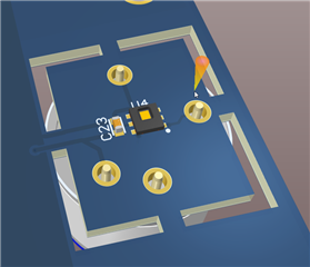
I am trying to measure the ambient temperature and humidity for example of a room, but due to the heat created on board during the charging of the battery, the temperature seems to be much higher. Is there anything that can be done on the PCB to isolate the heat transfer to the sensor? I am thinking the heat is being detected due to the connected GND plane

  • Hi Dharmesh,

    It is important to ensure that the humidity sensor is thermally isolated from any heat sources on the board, since heating will affect both the temperature and relative humidity measurement. Here are some PCB layout guidelines: 

    • Placed the humidity sensor as far away from any heat sources as possible, such as in the corner of the PCB, away from any power intensive board components (such as battery, display, or microcontroller). 
    • Eliminate copper planes under/near the sensor (especially if those copper planes are connected to heat-generating components).
    • Use slots, cutouts or perforation around the sensor to reduce thermal mass and obtain a quicker response time to environmental changes.
    • Leave the thermal pad floating (do not solder it down) to further reduce thermal mass.

    Please refer to this document for additional guidance: Optimizing Placement and Routing for Humidity Sensors

    Best regards,

    Sakeenah 

  • Hi

    Thank You for your reply.

    This is what we are now doing:

    We have done a PCB cutout around the sensor, with the exception of where traces will go through and on the either side/ 


    The GND and VCC layer copper is limit to the point where the cut out starts

    Is there any additional I could do?

  • Hi Dharmesh,

    These updates look pretty good! You can make the cutout around the HDC sensor smaller to save board space, we have examples with cutouts of diameter ~6mm. 

    What is connected under the HDC sensor, and what is JT1 connected to? 

    If you have placed the sensor far away from potential heat sources, you should be in good shape. 

    Best,

    Sakeenah

  • Hi 

    Below the HDC Sensor is the following sensor Temperature, Pressure and Humidity sensor PRHT-A1 - Alphasense -

    B2B is currently used in our design, but we plan to replace it with the HDC. We have included B2B as an alternative option, which we hope will not be necessary due to the HDC’s isolation.

    By making the cutout on the PCB smaller, wouldn’t that increase the likelihood of heat transfer?

  • Hi Dharmesh,

    I see, thanks for sharing that! Hopefully the PCB design updates will eliminate the heating issues. The current board looks pretty good. Do let us know if there are any additional problems and we can look into it, you can reopen this E2E or create a new one. 

    I also think we may have misunderstood each other about the cutout sizing! We have layout examples that have a cutout diameter of of ~6 mm - this is the board space surrounding the sensor (the red line I drew in the image below). I think what you have is fine though, so this is just a suggestion if you need to save some board space. Meanwhile, regarding the actual width of the cutout spacing between the PCB sections (the light blue line), we have examples that use ~30mils - increasing the width of this cutout will further help with thermal isolation, as well as any other methods to reduce thermal mass (such as perforation, placing the sensor on an offshoot of the PCB, using edge connectors to connect a smaller sensor PCB, etc.)

    Best,

    Sakeenah

  • HI

    Thanks

    This is the updated design. I have removed part of the PCB, as indicated by your red line. The spacing, as shown by the blue line, is approximately 62 mils.

    The trace widths for VCC and GND are 0.5mm, while the I2C signals are 0.3mm on the PCB. Would this be sufficient, or would we need to reduce the VCC and GND trace widths from 0.5mm to 0.3mm?   

  • Hi Dharmesh,

    I think your current trace width is fine, any effects from reducing it further would be negligible. The main requirement is to eliminate the nearby copper planes which you have already done. 

    Best,

    Sakeenah