Tool/software:
Hello TI Team,
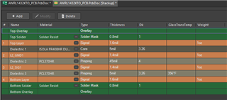
I am working with the TI reference design AWRL1432KTO and need to confirm the PCB layer stackup for manufacturing.
Specifically, I would like to know:
The number of layers in the PCB
The thickness of each layer (copper & dielectric)
The dielectric material and its properties (Dk, Df)
Since I do not have access to Altium Designer, I am unable to check the Layer Stack Manager in the .PcbDoc file.
Could you provide the default stackup details or share a fabrication drawing (if available)?
Thank you!