Other Parts Discussed in Thread: AWR1642
Tool/software:
Hello,I hope this message finds you well.
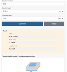
I am currently studying and analyzing the antenna structure used in the AWR1642 radar module. During my evaluation of the PCB layout and the stack-up data, I noticed some discrepancies compared to theoretical microstrip patch antenna dimensions typically calculated for 79.5 GHz operation using standard formulas (based on RO4350B, εr = 3.66, h = 0.1016 mm).
I would like to understand:
1. Why the patch dimensions in the AWR1642 PCB layout appear smaller than the theoretical values (e.g., W ≈ 1.236 mm, L ≈ 0.947 mm)?


2. Why the patch shapes are not purely rectangular—?

3. Why the spacing between series patches in the array is significantly below λ/2? (Based on εr = 3.66 and f = 79.5 GHz, λ/2 ≈ 0.935 mm)