This thread has been locked.

If you have a related question, please click the "Ask a related question" button in the top right corner. The newly created question will be automatically linked to this question.

MMWAVEICBOOST: MMWAVEICBOOST HDR60 pinouts

Part Number: MMWAVEICBOOST

Tool/software:

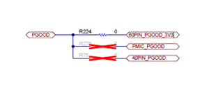
Hello! I am trying to create a list, or matrix of of connections between the two HDR60 connectors, J10 for the DCA1000 connection and J4 for LVDS and JTAG. I'm trying to establish which connections could be connected straight through, EG presumably RADAR_DP0-7 can be "jumped" or shorted together, skipping any additional circuitry on the BOOST board. However, which (if any) of the other connections can be connected 1:1, are required for the proper operation of the LRU connected to J4, and/or are unnecessary/incompatible with one another (EG J10.13 PGOOD is not a direct matchup with J4.14 60PIN_PGOOD_3V3)?

  • Elliot,

    Please allow me a couple of days to get back to you.

    Thanks,

    Swarnendu

  • Hello Elliot,

    Before answering your question, I would like to know the rationale behind this. Why do you want to short signals from these two connectors?

    Considering the signals that are shared by J4 and J10 and have the same net names are internally same. Hence no need to externally short. On the other hand, if you like to tie down or short let's say RS232/SPI/I2C signals, you can follow the MUX settings to do so. The MUX settings allow you to differentiate or connect different signals that share a same net at some point of the design.

    Considering the below default setting, 60PIN_PGOOD_3V3 is connected to the PGOOD by a 0ohm resistor. 

    So, my suggestion would be to use the MUX settings, if you want to connect the comm signals from one of these connectors to the other.

    Thanks,

    Swarnendu

  • Hello Swarnendu!

    Thank you very much for your response! I'm actually trying to create a new PCB starting with JUST the two connectors on it to reroute necessary signals. The current project I'm working on, the BOOST board has FAR more functionality than we need and we're trying to A) reduce the size & complexity of the PCB or, ideally B) Just replace the BOOST with a simple PCB rerouting the pins as necessary.

    Thank you

    Elliot

  • Elliot,

    Thanks for sharing the insights. I would like to have few additional queries based on the details you have provided:

    1. Which radar device you are working with?

    2. If you could share more about the necessary functionality you require, we might be able to point you to simpler development purpose boards compared to the BOOST board based on the primary IC you are using.

    3. I understand that you are trying to achieve a simpler evaluation PCB. In that case, if you do not want the MUXING provisions available in the BOOST board for the desired signals, you can tie up the signals in your PCB. However, if your mean to communicate to the primary IC is still the BOOST board, you may get conflicts if the MUX settings are not aligned properly. If my understanding is correct, I would like you to track the required signals to the respective MUXs and decide how you would like to set the MUX setting.

    Thanks,

    Swarnendu