


Tool/software:
HI Ti experts
We converted the layout file of the AWRL6844EVM provided by TI into a .brd file that can be read by Allegro.
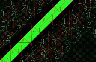
However, we noticed a large number of DRC errors in the antenna area related to the VIAs. We're wondering if this issue was caused by the file conversion process.
In addition, we observed that the VIA symbols extend beyond the boundary and into the area between the trace and GND. This issue doesn’t appear in the PROC182A_PCBlayers.PDF document.
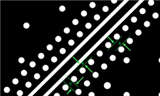
Since we would like to understand the correct spacing arrangement of these VIAs, would it be possible for you to provide the dimensions labeled A, B, and C in the image for our reference?
-
A: Spacing between VIAs (front-to-back)
-
B: Distance from VIA to boundary
-
C: Spacing between VIAs (left-to-right)
BR,
Vincent
