This thread has been locked.

If you have a related question, please click the "Ask a related question" button in the top right corner. The newly created question will be automatically linked to this question.

IWRL6432AOP: an additional design requirement

Part Number: IWRL6432AOP
Other Parts Discussed in Thread: IWRL6432, , IWR6843AOP, IWR1843AOP

Tool/software:

Hi expert,

The customer has previously evaluated the IWRL6432 and intended to use the AOP version.

However, they have now found that while the IWRL6432AOP is identical to the IWRL6432 in terms of principle and packaging, an additional design requirement has been introduced, which will significantly increase the difficulty of routing.

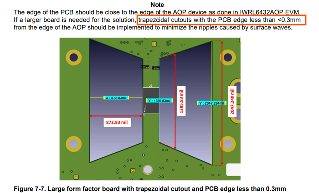
Since this requirement was not included in the original reference design, they would like to know the reason for adding it. In addition, as no clearance is reserved on the official website's development board, they also want to confirm whether this new requirement is put forward due to related issues.

Could you help answer their question?


Best regards,

Winnie

  • Hi,

    An expert will comment shortly.

    Best,

    NAte

  • Winnie, 

    The change was made to document best practices to achieve best device performance. These design requirements are also seen on our IWR6843AOP and IWR1843AOP.

    It is possible for many customers to disreguard the the trapezoidal cut outs requirments. Doing so will result in riples in the antenna radiation pattern at the FoV extremes. Most custumers will not notice this as it will only be problematic at large incident angles (low grazing angles) and long distances wrt the radar. 

    I hope this helps!

    Thanks 

    Blake

  • Hi Blake,

    The EVM of IWRL6432aop has exposed copper with a stencil opening. If this part presses against the chip, it may lift the chip up (since there seems to be a raised die under the chip). If it doesn't press against the chip, it serves no purpose. How is this design considered?

    This feature is not present on the package, and its position is also offset.

    Best regards,

    Winnie

  • Hi Winnie! Happy Wednesday! 

    This question is a new question and not related to the previous one. In the future, please start new threads with new questions as this helps searchability for other E2E users. 

    The copper area is not expected to make contact with the die. However, contrary to your assertion, it does play a role. The exposed pad allows for improved cooling of the die by creating a surface for heat to radiate from the die to the PCB. These ground planes then dissapate the heat. 

    I hope this helps with your design! 

    Respectfully, 

    Blake