This thread has been locked.

If you have a related question, please click the "Ask a related question" button in the top right corner. The newly created question will be automatically linked to this question.

TMP119EVM: Changing I2C address on the TMP119 EVM board

Part Number: TMP119EVM
Other Parts Discussed in Thread: TMP119,

Tool/software:

Hi,

I'd like to have support on the TMP119 EVM board.

https://www.ti.com/tool/TMP119EVM

I'd like to connect two of these sensors to my MCU detaching the sensor part from the rest of the USB dongle and adding a pin strip.
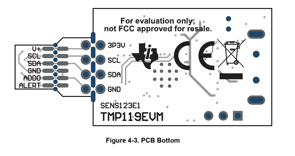
Based on the documentation provided, the ADD0 pin on this board is tied to GND:


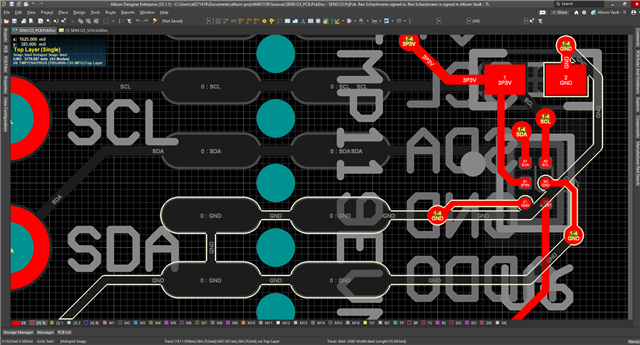
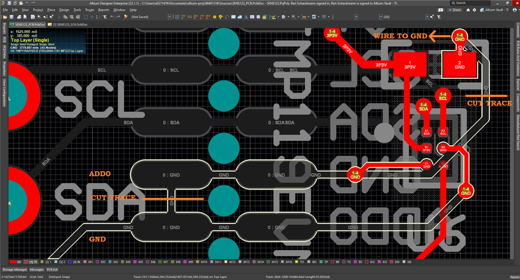
To change address on one of the two sensors I cut the trace between ADD0 and GND on the PCB:

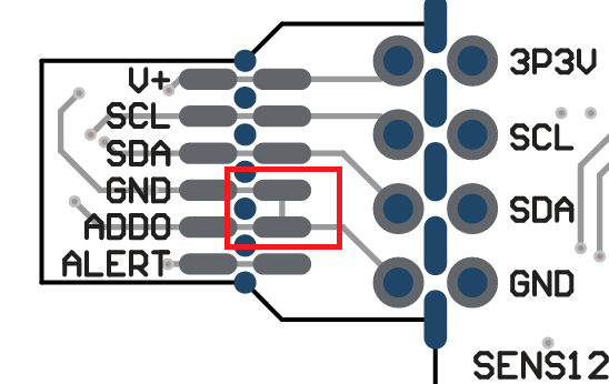
then I soldered a wire on the GND pad while the original GND pin on the 4 way header is the new ADD0:

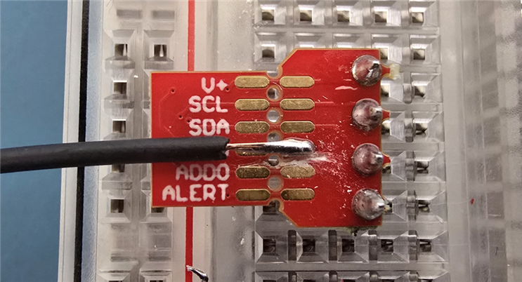
Now if I connect the newly created ADD0 pin on the 4-way pin strip to GND as in the original board, everything works fine and the TMP119 has the 0x48 I2C address.

If I connect ADD0 to V+ (3.3V in my case) I would like to assign the 0x49 address to the TPM119 but it doesn't work and there's a significant current draw (>100mA) on the 3.3V supply.
I've double checked with a multimeter that GND and ADD0 are NOT short circuited on the board anymore, so my hardware modification seems to be fine.

But I can't explain the behaviour, I've also thought about a ESD damage to the ADD0 pin but I was grounded when I made this modification, also the chip continues to work correctly when I connect ADD0 to GND.

Could you help me with this?

Is there another way I can try to change to I2C address of the TMP119 using the EVM?

Thank you for your support!

  • Hi Frank,

    It looks like you've attached your wire to the GND pin, not the ADD0 pin. Try moving it over to ADD0 before plugging it into V+.

    I'm glad to see you're making use of your perforated EVM PCB. We often make these features and don't get to know if people really like them or use them.

    ren

  • Hi Ren,

    thank you for your reply.

    I think that's correct.

    The wire is attached to GND, the pin on the 4-way header that was originally labeled as GND it's now ADD0. 
    So I connect the black wire to GND and I connect the ADD0 pin to either GND or V+ using a breadboard.

    If you look at the layout of the board what's labeled as GND on the circular through hole pad, it's actually connected to ADD0 which is in turn short cirucited to GND.

    So I think we're back to square one...I don't know why it's not working :/

  • I understand. The PCB is mislabeled. C1 is the ADD0, and the trace connects it to the pad labeled GND. Sorry for this mix-up.

    The C1 pin is also connected to the bypass cap. Moving your wire from GND to V+ should charge and discharge this cap, but there shouldn't be harm in having it tied off. I have to assume you have damaged your TMP119 at some point in your rework; perhaps even at the hands of this discharging cap. I'd like to get you a replacement TMP119EVM, but there is a risk of the same issue popping up again. You may need to remove the cap first, or cut its trace as well and rewire it to actual GND.

    If you're not able to request a sample EVM from https://www.ti.com/tool/TMP119EVM#order-start-development then please send me your address in a private message. I will have one shipped to you.

    Thanks for your understanding,

    ren

  • Hi Ren,

    thank you for your help.


    So basically the ADD0 label on the board should be actually GND while the GND pad where I soldered my wire is connected to the GND of the bypass capacitor and the ADD0 pin of the TMP119.

    With the modification I made, trying to connect ADD0 to 3.3V to change address to 0x49,  I actually put the TMP119 GND to 3.3V (same as V+ so the chip is not powered) while ADD0 was put to GND, so the ADD0 pin had to withstand a negative 3.3V on it...

    When I did this I measured a current over 100mA, does the detachable part of the board has an internal GND plane or ground fills?
    It doesn't seem that at least the latter is the case based on a visual inspection.
    With no GND internal planes and no GND fills basically the only part that was negatively polarized was the TMP199 ADD0 pin, but a >100mA current flowing in the IC through ADD0 seems enough to burn the IC... that not only hasn't happened but the chip actually works well when I restore the original configuration with ADD0 to GND.

    Where do you think this short circuit-like current is flowing?

    About the replacement board I need to talk with my colleagues since I'm using this chip at work for a project, so I'll let you know as soon as we make a decision, thank you for the availability.

    In the meantime, could it be worth to try to do another modification on the EVK I already have since the chips seems to be still working?
    The correct mod should be like this right?

  • It would have to be your ADD0 pin that has burned a path to GND in the IC. The input may still function, but this low resistance to GND prevents you from tying the pin to anything other than GND. In failure analysis, we would curve trace the pins; comparing leakages of each pin to a known good device. This would confirm the new current path. The ICs are always damaged at these "input cells." They are rarely damaged in the internal circuitry. This is why your IC still works otherwise.

    I suspect your IC has this damage, because there isn't anything else on that section of PCB to cause the short. There are no internal layers in that section of the PCB, as you have surmised. It could be that your trace cut was not thorough, but you claimed to have confirmed it. When I cut a trace, I like to cut it on both sides and lift out a piece of the copper between. It looks to me like you have done such a job. The trace was designed to facilitate such a cut, as well. The intention with the design was to enable you to do exactly what you did. 

    To be clear, I'm not asking for a return of the board you're using. I'm offering a free replacement at no cost as compensation for your troubles. I have revised this design to correct the mistake, but it will be a while before we see the revision stocked.

    Finally, yes, what you have drawn is the correct modification. In my revision, I swapped the ADD0/GND labels just as you did and I connected the capacitor's GND trace to the B2 pin's trace/via.

    thanks,

    ren

  • Ok Ren, it's all clear.

    Thank you for the help.
    Since this experience was somehow useful to create a board revision, as I user I think it would nice to have the possibility in the EVK to change I2C address without cutting and soldering stuff manually, although it would be obviously a bigger design effort than changing labels.

    I'll send you an address to get a new free sample in private.

    Thanks!

    Francesco