This thread has been locked.

If you have a related question, please click the "Ask a related question" button in the top right corner. The newly created question will be automatically linked to this question.

AWR6843: hardware design

Part Number: AWR6843

Tool/software:

Hi,

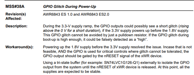
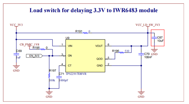
I am studying the design of the AWR6843ISK-ODS and noticed that the VIOIN power supply goes through the U9 switch. However, when I checked the AWR6843 datasheet, I didn’t find any special requirements for the VIOIN input power sequencing.

What is the function of the U9 switch chip? Is it necessary? Looking forward to your reply.

Best, 

Yunlong 

  • Hi Yunlong,

    Thanks for posting your question over E2E. Please allow us to respond in a working day or two.

    Best regards,
    Deexith.

  • Hi Yunlong,
    I apologize for the delay in response. No additional delay is required for 3.3V rail (delay switch can be removed). You can follow the datasheet.

    However, please also consider the errata mentioned below


    During the 3.3-V supply ramp, the GPIO outputs could possibly see a short glitch (rising above the 0 V for a short duration), if the 3.3V supply powers up before the 1.8V supply.
    There is no issue If the GPIOs are not used for any critical signaling (e.g : CAN PHY Enable) where glitches can be tolerated. .
    If GPIOs are used for any critical signaling I would recommend to use a tri-state buffer and/or external pull-ups/pull-downs on it.

    Thanks,
    Sivaprasad