


Other Parts Discussed in Thread: TDC7200
Tool/software:
Hi,
I am using the TDC1000 connected with an STM32 for water and gas level measurement. I have configured the TDC1000 registers based on the datasheet. However, my sensor behaves differently from what I have set in the TDC1000 registers. I am using a 1 MHz transducer, and I am getting multiple STOP pulses per measurement cycle from the TDC1000, even though my configuration is set for single echo mode with NUM_RX = 1h (expecting only 1 STOP pulse). I have also set NUM_TX = 1h (1 pulse), but the TX pin outputs 5 pulses (default value, 5h), even when I change the number of pulses in the register.
I have provided a 16 MHz CLKIN to the TDC1000. I also have another question: how should I choose TX_FREQ_DIV in the CONFIG_0 register based on the transducer frequency? Currently, I am using the default setting, and I don’t observe any difference in the STOP pulse and COMPIN signals when I measure water level in a white glass beaker.
Below, I have provided the circuit diagram and register settings and the signals I obtained from the TDC1000 IC when the 1 MHz transducer was connected.
Register Setting of TDC1000:
CONFIG_0 Register
-
TX_FREQ_DIV = 2h: Divide by 8 (default)
-
NUM_TX = 1h: 1 pulses
CONFIG_1 Register
-
NUM_RX = 1h: 1 event (1 STOP pulse output)
-
NUM_AVG = 0h: 1 measurement cycle (default)
-
RESERVED = 1h: Reserved (default)
CONFIG_2 Register
-
TOF_MEAS_MODE = 0h: Mode 0 (default)
-
CH_SEL = 0h: Channel 1 (default)
-
EXT_CHSEL = 0h: Disable external channel select (default)
-
CH_SWP = 0h: Disable automatic channel swap (default)
-
DAMPING = 0h: Disable damping (default)
-
MEAS_MODE = 0h: Time-of-flight measurement (default)
-
VCOM_SEL = 1h: External
CONFIG_3 Register
-
ECHO_QUAL_THLD = 4h: –220 mV
-
BLANKING = 0h: Disable power blanking (default)
-
TEMP_CLK_DIV = 0h: Divide by 8 (default)
-
TEMP_RTD_SEL = 0h: PT1000 (default)
-
TEMP_MODE = 0h: Measure REF, RTD1 and RTD2 (default)
-
RESERVED = 0h: Reserved (default)
CONFIG_4 Register
-
TX_PH_SHIFT_POS = 1Fh: Position 31 (default)
-
TRIG_EDGE_POLARITY = 0h: Rising edge (default)
-
RECEIVE_MODE = 0h: Single echo (default)
-
RESERVED = 0h: Reserved (default)
TOF_1 Register
-
TIMING_REG[9:8] = 0h: 0 (default)
-
LNA_FB = 1h: Resistive feedback
-
LNA_CTRL = 0h: Active (default)
-
PGA_CTRL = 0h: Active (default)
-
PGA_GAIN = 7h: 21 dB
TOF_0 Register
-
TIMING_REG[7:0] = 0h: 0 (default)
ERROR_FLAGS Register
-
ERR_SIG_HIGH = 0h
-
ERR_NO_SIG = 0h
-
ERR_SIG_WEAK = 0h
-
RESERVED = 0h: Reserved (default)
TIMEOUT Register
-
TOF_TIMEOUT_CTRL = 3h: 1024 × T0
-
ECHO_TIMEOUT = 0h: Enable echo timeout (default)
-
SHORT_TOF_BLANK_PERIOD = 4h: 128 × T0
-
FORCE_SHORT_TOF = 0h: Disabled (default)
-
RESERVED = 0h: Reserved (default)
CLOCK_RATE Register
-
AUTOZERO_PERIOD = 0h: 64 × T0 (default)
-
CLOCKIN_DIV = 0h: Divide by 1 (default)
-
RESERVED = 0h: Reserved (default)
Configuration Data Values
CONFIG_0_DATA = 0x41;
CONFIG_1_DATA = 0x41;
CONFIG_2_DATA = 0x80;
CONFIG_3_DATA = 0x04;
CONFIG_4_DATA = 0x1F;
TOF_1_DATA = 0xE4;
TOF_0_DATA = 0x00;
ERROR_FLAGS_DATA = 0x00;
TIMEOUT_DATA = 0x23;
CLOCK_RATE_DATA = 0x00;
Circuit Diagram: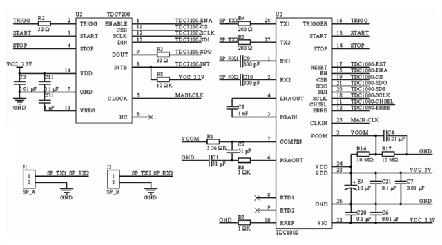
1.Trigger signal

2.Start Pulse From TDC1000
3.Stop Pulse from TDC1000
4.COMPIN signal from TDC1000 
5.Signal From TX and RX pin of TDC1000 
