PGA970: Programming a binary over SPI

Part Number: PGA970

Tool/software:

We would like to program a custom binary to the PGA970 over SPI. My understanding from the datasheet is that FRAM can be programmed from SPI when in reset. My questions are:

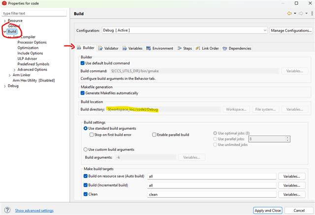
  • How do I generate a binary file from CCS? We've built and flashed the example program with the XDS200 debugger.
  • What address do I program the binary file to?
  • Hi Nathan, 

    Welcome to E2E! You are correct, the device must be in reset to program the FRAM over SPI. Just as a note - these instructions are for CCS v12.8. If you're using a different version of CCS, it may look a bit different. 

    To generate a binary file, you need to go to "Projects --> Properties". You'll get a dialog that looks like the following:

    Go to the "Build" tab, and you can configure the settings for the output files. You can see in this screenshot that my build files will be generated in the project's "Debug" folder. Once you have the settings configured, you can compile your code, and the output files will be generated.

    If you are using the example firmware, then you should have the .gel file ("docs" folder in the CCS project) which you can use to create a .ccxml file for flashing. You can copy the .gel file to your preferred directory and use it for any firmware you write. You just need to make sure it is linked to whatever Target Configuration file you use when you're flashing.

    I believe the .gel file that comes with the generic firmware maps to the DEVRAM. You need to open to .gel file and make sure the highlighted portion matches:

    If the highlighted portion reads 0x01 instead of 0x00, then you will map you code to DEVRAM. If it reads 0x00, then it will map to FRAM.

    Once you have your .gel and .ccxml files setup correctly, then you can flash the firmware as normal.

    Let me know if this helps.

    Thanks,

    Maggie