

Other Parts Discussed in Thread: PGA970, , UNIFLASH
Tool/software:
Once I have written firmware, and I am ready to flash it to PGA900 or PGA970, what tool should I use?

This thread has been locked.
If you have a related question, please click the "Ask a related question" button in the top right corner. The newly created question will be automatically linked to this question.
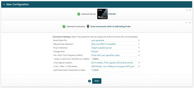
Uniflash is TI's preferred tool for flashing firmware to PGA900 and PGA970.
The XDS110 debugger (which can be found on any MSP launchpad or bought separately) is TI's preferred debug probe. This example uses an XDS110.
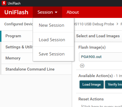
The user can save their session configuration settings.
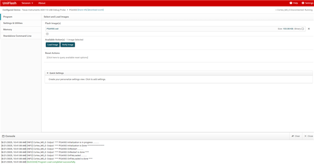
The default settings in Uniflash will flash firmware to the PGA900/970 DEVRAM. If the user would like to flash their firmware to the OTP (PGA900) or FRAM (PGA970), they must change the .gel file. In the .gel file, the remap function sets the REMAP address to 0x01:
Config_Remap()
{
   WR_MEM_08(REMAP_ADDR,0x01);
}
This must be set to 0x00 if the user wants to write to OTP or FRAM.
//####################################################
//PGA900 OTP GEL file
//v1.1 March 4,2014
//####################################################

//*******************************************************************
//Watchdog register
//*******************************************************************
#define WDOG_CTRL_STAT_ADDR (0x4000051C)

//*******************************************************************
//Remap register
//*******************************************************************
#define REMAP_ADDR (0x40000220)

//*****************************************************************************
//Read write prototype
//*****************************************************************************
#define WR_MEM_08(addr, data) *(unsigned char*)(addr) = (unsigned char)(data)
#define RD_MEM_08(addr)       *(unsigned char*)(addr)

//*****************************************************************************
//Global Functions
//*****************************************************************************

//Watchdog is disabled to eliminate warm resets during debug
Disable_Watchdog()
{
   WR_MEM_08(WDOG_CTRL_STAT_ADDR,0x00);
}

//Set the processor to User mode after a file is loaded, on a
//restart or on a reset
//This will facilitate code loading and debug by putting the processor in a known
//state

PGA900StartState()
{
   xPSR = (xPSR & ~0x1F) | 0x10;
}

OnFileLoaded()
{
   GEL_TextOut("****  PGA900 OnFileLoaded .......... \n","Output",1,1,1);
   PGA900StartState();
   Config_Remap();
   GEL_TextOut("****  PGA900 OnFileLoaded is done **** \n","Output",1,1,1);
}

OnRestart()
{
   GEL_TextOut("****  PGA900 OnRestart .......... \n","Output",1,1,1);
   PGA900StartState();
   Config_Remap();
   GEL_TextOut("****  PGA900 OnRestart is done **** \n","Output",1,1,1);
}

OnReset()
{
   GEL_TextOut("****  PGA900 OnReset .......... \n","Output",1,1,1);
   PGA900StartState();
   Disable_Watchdog();
   Config_Remap();
   GEL_TextOut("****  PGA900 OnReset is done **** \n","Output",1,1,1);
}

Config_Remap()
{
   WR_MEM_08(REMAP_ADDR,0x00);
}

OnTargetConnect()
{
   GEL_MapOff();
   GEL_MapReset();
   GEL_MapAddStr(0x00000000, 0, 0x00002000, "RAM|AS4", 0);  // OTP
   GEL_MapAddStr(0x21000000, 0, 0x00002000, "R|W", 0);  // Development RAM
   GEL_MapAddStr(0x20000000, 0, 0x00000400, "R|W", 0);  // SRAM Internal
   GEL_MapAddStr(0x40000000, 0, 0x00000080, "R|W", 0);  // EEPROM
   GEL_MapAddStr(0x40000080, 0, 0x00000008, "R|W", 0);  // EEPROM Cache
   GEL_MapAddStr(0x40000088, 0, 0x00000578, "R|W", 0);  // Control and status registers
   GEL_MapAddStr(0xE000E000, 0, 0x00000F00, "R|W", 0);  // M0 registers
   GEL_MapOn();
   PGA900StartState();
   GEL_TextOut("****  PGA900 Initialization is in progress .......... \n","Output",1,1,1);
   Disable_Watchdog();
   Config_Remap();
   GEL_TextOut("****  PGA900 Initialization is Done ****************** \n","Output",1,1,1);
}

OnPreFileLoaded()
{
    GEL_TextOut("**** PGA900 OnPreFileLoaded .......... \n","Output",1,1,1);
    Config_Remap();
    GEL_TextOut("**** PGA900 OnPreFileLoaded is done **** \n","Output",1,1,1);
}//####################################################
//PGA970 FRAM GEL file
//v1.0 May 15,2015
//####################################################
//*******************************************************************
//Watchdog register
//*******************************************************************
#define WDOG_CTRL_STAT_ADDR (0x4000051C)
//*******************************************************************
//Remap register
//*******************************************************************
#define REMAP_ADDR (0x40000220)
//*****************************************************************************
//Read write prototype
//*****************************************************************************
#define WR_MEM_08(addr, data) *(unsigned char*)(addr) = (unsigned char)(data)
#define RD_MEM_08(addr) *(unsigned char*)(addr)
//*****************************************************************************
//Global Functions
//*****************************************************************************
//Watchdog is disabled to eliminate warm resets during debug
Disable_Watchdog()
{
WR_MEM_08(WDOG_CTRL_STAT_ADDR,0x00);
}
Config_Remap()
{
WR_MEM_08(REMAP_ADDR,0x00);
}
//Set the processor to User mode after a file is loaded, on a
//restart or on a reset
//This will facilitate code loading and debug by putting the processor in a known
//state
PGA970StartState()
{
xPSR = (xPSR & ~0x1F) | 0x10;
}
OnFileLoaded()
{
GEL_TextOut("**** PGA970 OnFileLoaded .......... \n","Output",1,1,1);
PGA970StartState();
Config_Remap();
GEL_TextOut("**** PGA970 OnFileLoaded is done **** \n","Output",1,1,1);
}
OnRestart()
{
GEL_TextOut("**** PGA970 OnRestart .......... \n","Output",1,1,1);
PGA970StartState();
Config_Remap();
GEL_TextOut("**** PGA970 OnRestart is done **** \n","Output",1,1,1);
}
OnReset()
{
GEL_TextOut("**** PGA970 OnReset .......... \n","Output",1,1,1);
PGA970StartState();
Disable_Watchdog();
Config_Remap();
GEL_TextOut("**** PGA970 OnReset is done **** \n","Output",1,1,1);
}
OnTargetConnect()
{
GEL_MapOff();
GEL_MapReset();
GEL_MapAddStr(0x00000000, 0, 0x00004000, "R|W", 0); // FRAM_TEXT
GEL_MapAddStr(0x21000000, 0, 0x00004000, "R|W", 0); // Development RAM
GEL_MapAddStr(0x20000000, 0, 0x00000800, "R|W", 0); // SRAM Internal
GEL_MapAddStr(0x20000800, 0, 0x00000200, "R|W", 0); // Waveform RAM
GEL_MapAddStr(0x40000000, 0, 0x000005E7, "R|W", 0); // Control and status registers
GEL_MapAddStr(0xE000E000, 0, 0x00000F00, "R|W", 0); // M0 registers
GEL_MapOn();
PGA970StartState();
GEL_TextOut("**** PGA970 Initialization is in progress .......... \n","Output",1,1,1);
Disable_Watchdog();
Config_Remap();
GEL_TextOut("**** PGA970 Initialization is Done ****************** \n","Output",1,1,1);
}