Other Parts Discussed in Thread: TMP116
Tool/software:
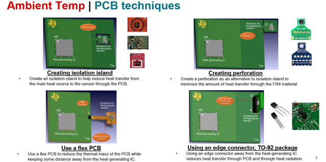
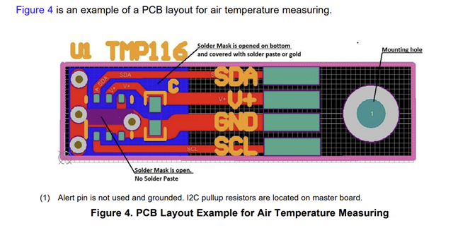
I am using the TMP117 to measure moving air temperature. I would like to optimize the layout of the chip and surrounding area to have the highest precision and response time for measuring the environment. In the datasheet of the TMP117 it says you should not solder the thermal pad on the IC. In SNOA986A Precise Temperature Measurements With the TMP116 and TMP117, there is an image of a layout for air temperature measurements on page 8 which shows the pcb area under the thermal pad exposed to a ground copper trace through the solder mask cut out.
What is the correct layout to follow for my application? Should I have copper planes next to and under the IC with solder mask removed or not? Should the thermal pad be touching exposed copper but just not soldered? Or should the thermal pad just be isolated from the pcb altogether with solder mask covering that area?