LMT86: Layout Guidelines of SC70

Part Number: LMT86

Tool/software:

In LMT86 datasheet, there is a Layout Guidelines as following fig.

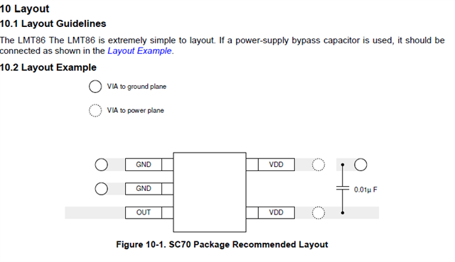
In my understanding, the optimal connection order from a low-noise perspective is: IC's VCC pin → decoupling capacitor → via → VCC layer.
However, your recommendation seems to reverse the order of the capacitor and the via.
Could you please clarify the reasoning behind this approach?

BR

  • Toshio,

    You are correct in your understanding, the bypass capacitor should be as close as possible to the LMT86 without vias in between. I think this layout drawing is misleading in that aspect. I am not sure how much a difference it will make but I would have the via to the power plane come after the bypass cap connects to the VDD pin, not before. I will look into if our team can update this drawing.

    Thank you

    -Alex Thompson

  • Dear Alex,

    Thank you for your reply and advises.
    My question was cleared.
    We are appreciated your help.
    Thank you so much.

    BR