


Tool/software:
Hi Ti,
As our project progresses, we have some questions regarding firmware flashing that we would like to consult with you about.
We understand that the architecture of the EVB is as shown in the attached diagram, which includes the XDS110 and FTDI on the 6844 EVB PCB.
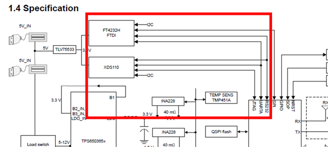
Due to size constraints, we have removed the XDS110 and FTDI from our custom PCB. We would appreciate your guidance on the following questions:
- Is it possible to use the XDS110 Debug Probe or the MMWAVEICBOOST to upload firmware?
- Would you recommend using UART or JTAG for firmware uploading?
- Does the RESET pin need to be connected to the XDS110 Debug Probe, or can it be configured as a button?( Similar to 6844)
- For firmware uploading, would you recommend using the default visualizer or the arprog_cmdline_6844.exe tool?
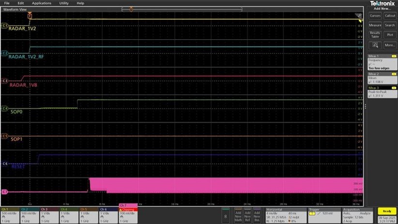
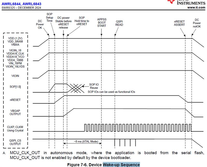
- The left side of the attached figure shows the measured Wake-up Sequence of our custom PCB, which has slight differences compared to the Reset signal shown on the right side. Will this differences cause any issues?
Thank you
ED
