


Part Number: AWR2944EVM
Hi,
at the EVM PCB arround the antenna there is a large clean of elements area:
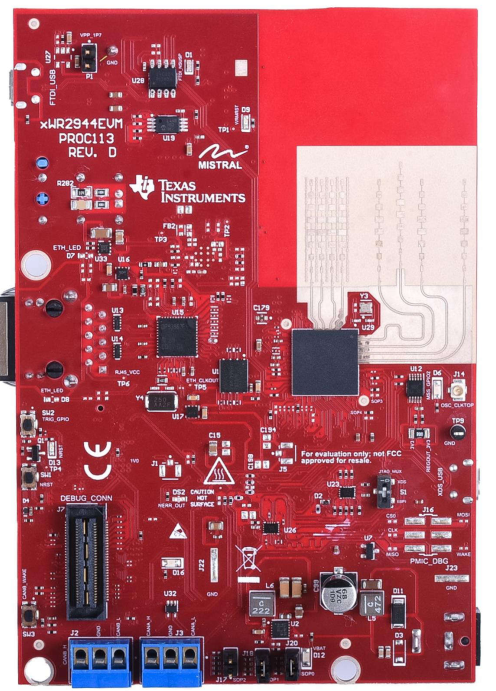
Please explain why it is needed and what is the minimal required size of such area for our prototype PCB design
Kind regards,
Arie
Part Number: AWR2944EVM
Hi,
at the EVM PCB arround the antenna there is a large clean of elements area:
Please explain why it is needed and what is the minimal required size of such area for our prototype PCB design
Kind regards,
Arie


