


Part Number: TMP110
Other Parts Discussed in Thread: TMP1075
Hi,
Currently, we have considered TMP110D0IDPWR in using proto development in a application which runs on loop powered device. For evaluation, we had used the EVM kit and completed the functional validation. This part meets our current consumption requirement and now we are planning to incorporate this sensor in our PCB. During PCB design phase, we are facing few challenges mainly due to DFM constraints - PCB fabricator require min 5mils tolerance between pad to pad on a copper thickness of 2 oz/70microns finished thickness. We can't reduce the cu thickness as this is a 2 layer PCB designed for thermal dissipation.
- Can we remove this 0.1mm via in pad#3. We are connecting this pin directly to GND pad, as we do not intend to use ALERT functionality. Do you see any reliability issue if we don't use this via?
- Alternatively, can we leave this pin floating, as we don't use the Alert functionality.
- In the below example land pattern - typ exposed metal clearance is only 0.21mm. Can we consider the same value with respect to all the pads, please confirm.
- Alternatively, we are thinking to go with other equivalent part, for example - TMP1075DSGR. Could you please check on the peak current consumption of this part and confirm the specs are similar to the TMP110 series parts.
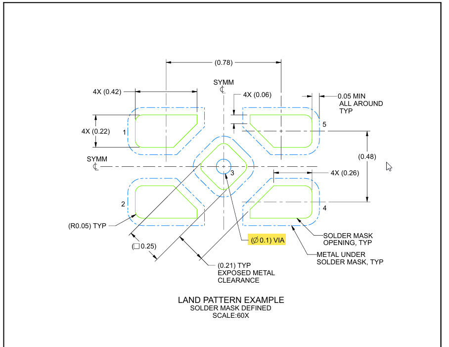
Please let me know if you require more details to clarify the above.
Best Regards,
Rajesh
