This thread has been locked.

If you have a related question, please click the "Ask a related question" button in the top right corner. The newly created question will be automatically linked to this question.

TMP300 temperature switch.

Other Parts Discussed in Thread: TMP300

Hello 

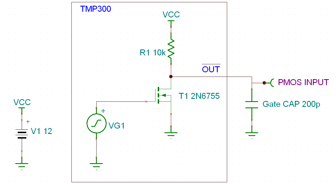
We have used TMP300 temperature switch.

We are tested the device and have some technical issue. We need to set temperature threshold @ -20 deg cel to make heater ON.

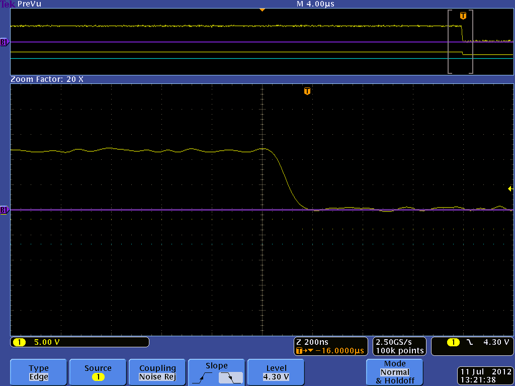
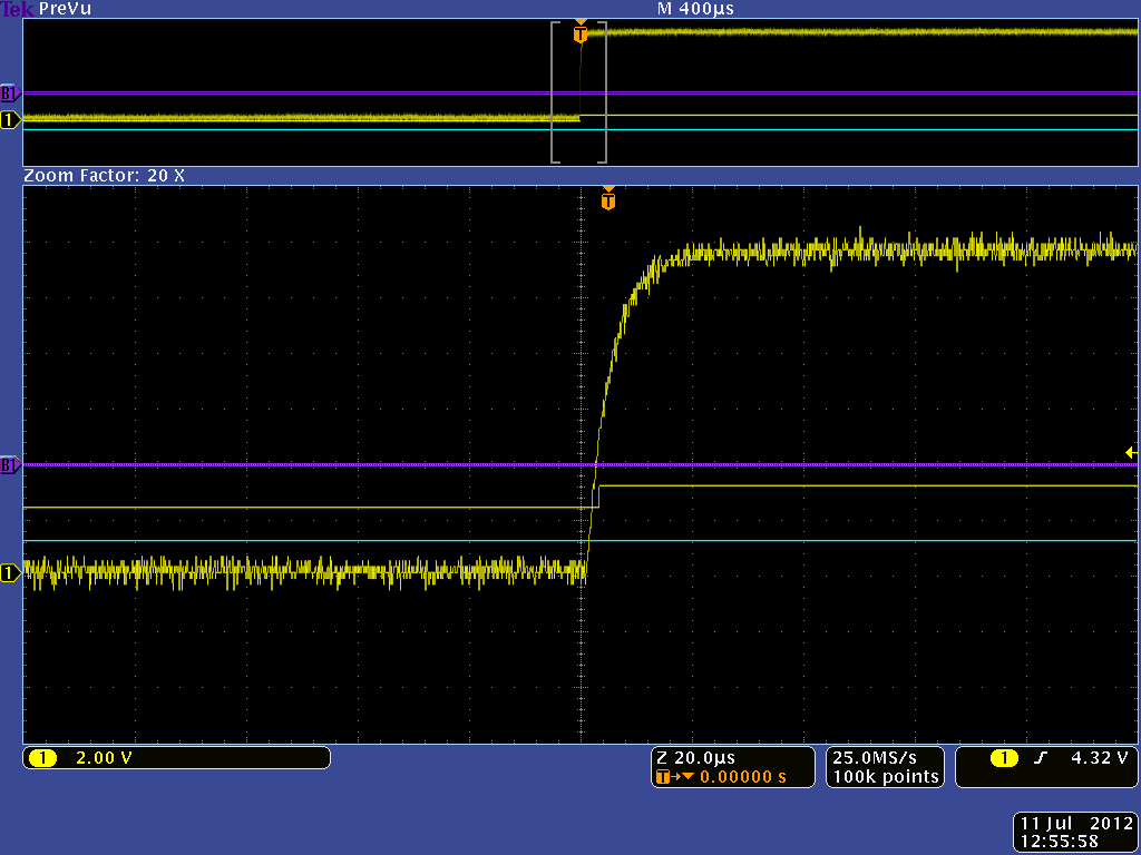
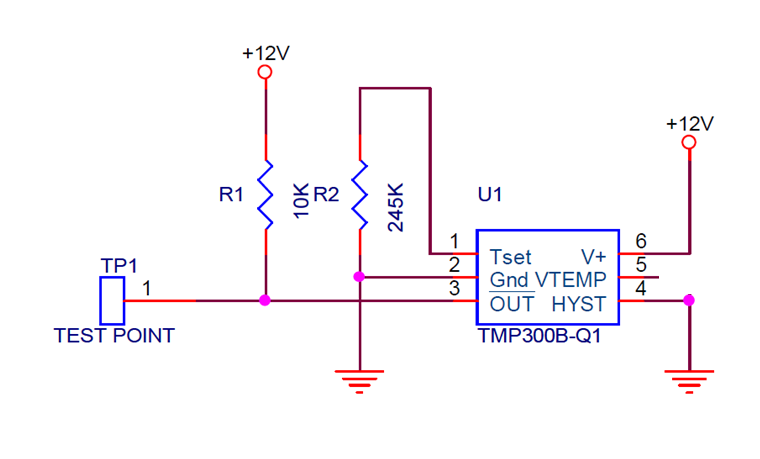
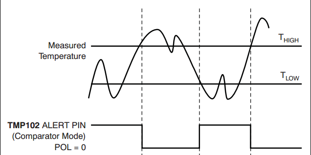
For testing we set temperature to 18 to 25 deg cel using Rset resistor.  According to data sheet and our understanding out# (pin 3) should go low (sharp falling) once set temperature is reached. But what we found is falling high to low is very slow,  just like some analog signal. For your reference I have attached the schematic used for testing.

Kindly suggest if it is correct or any modification required in it.

We need this temperature switch to control the heater ON/OFF. Whether this chip is suitable for such application or you have better solution.

Again, can this chip able to drive PMOS with Imax of 3A.

Kindly clarify.

  • Kumar,

    I am currently looking into this and will get back to you shortly.

  • Kumar,

    Can you please attach the schematic you have referenced. 

  • Hello Chris,

    We have used this Schemaitc and found that , it is working for positive temp @30*c but what we should do to get working this device for -20*C

    From Data sheet , we know it will be operational temp -40 to 150*c


    Pl send ur comments at earliest


    regards

    prem


    Sch_TMP300B-Q1.pdf
  • Prem,

    I don't see anything wrong with the schematic. You asked before whether the TMP300 is capable of driving a PMOS load. The answer is no. The OUT pin is an open drain and is not buffered. You would have to buffer the output in order to drive the large gate capacitance. When you see the signal falling slowly, is the device connected to the PMOS device? 

    Can you provide an oscilloscope shot showing this behavior with the time per division shown? This will help us better understand how fast the output is driven low. 

  • Prema,

    I have modeled your setup with the output pin driving a capacitive load. This capacitive load is a typical Cgs (Gate source capacitance) for a PMOS that can handle the kind of current you have referenced. You can see below that the output will not immediately transition from a high to a low with this load. As this capacitance is increased the fall time increases as well. My recommendation is to drive the PMOS through a buffer.


  • dear Chris,


    We had tested the TMP300 output without MOSFET drive, only with external pull up.

    The output is checked on Digital multimeter. The rate of falling was quite slow(in sec).

    If TMP300 can't work at negative temperature can you suggest any other temp switch from TI which will work at threshold -15/-20 deg cel.


    regards,

    prem

  • Prem,

    I will check the device with the setup you have provided at negative temperatures and see if I run into the same issue. If you could provide the board layout then that would be useful in determining if we are dealing with any parasitic effects that could cause this behavior.

  • Dear Chris,


    Thank you very much.

    My project is on hold due to this issue. your early reply is realy appreciated.

    prem


  • Prema:

    On the schematic you sent, pin 5 VTEMP is shown connected to ground. I do not believe this will allow the part to function properly.

    Please refer to Figure 14 of the data sheet TMP300B-Q1, SBOS586, and try that configuration.

    Thanks

    Mark

  • Prem,

    I agree with Marks assessment. I was successfully able to trip the output when I disconnected the Vtemp pin from ground. When this pin was at ground I was not able to trip the device at all. I set the TMP300 in the same configuration you provided in your schematic with Vtemp floating. You can see that when the device trips the fall time is around 200ns.

    Device is warmed up to trip output:

    Device is cooled off to un-trip output:

    Figure 14 recommends using bypass capacitors on pins Tset and Vtemp. These should be 0.01uF. You should also add a bypass capacitor of 0.01uF to the power supply to ground. These bypass capacitors should be placed as close to the pins as possible with very short leads. Preferably you would use surface mount devices.

  • Dear Mr. Chris Featherstone,

    The schematic which I have send to you, is without bypass capacitors. Earlier we checked with bypass capacitor that time I was not able to see any downfall at output.

    Temp set was -25 deg Cel. and We were trying to cool the temperature switch using "ICE bag". But we don't know exactly whether temperature is really reaching to -25 deg cel or not.

    Well, I would like to know, the above captured waveforms are for what temperature set. 

    And if it is on negative side, how you have subjected IC in negative temp environment.

    I will try again with pin 5 floating and/or with by pass capacitor and update you the result.

    Thanking you,

    Regards

  • Prem,

    This is what I used during my tests.

    TMP300 Configuration:

    I used M.G. Chemicals Super Cold 134 Plus as well as Thermal Cool hot and therapeutic pad from walgreens and obtained the same results above. The Super Cold spray reaches temperatures of -51oC as seen below. This was sprayed on the device package.  The thermal cool pad was placed in the freezer for 5 hours. The pad reached 32oF or 0oC. I placed the pad on the device package and ground lead in two separate tests.

    Super Cold Spray:


    Thermal Cool Pad Cold retention properties:


  • Dear Mr. cheris,

    We have tested the circuit with pin 5 floating and with bypass cap too. The output is tripping.....

    But I have a doubt.....As shown in datasheet....pin 3 (OUT#) is a active low pin...which means...it should be high @ normal condition and should go low when set temperature is reached.

    We have observed something reverse. (Which is actually same as the waveforms that you have attached)

    1. At room temperature (T> Tset) Vout=0.028V (Low)

    2. After cooling (when T<Tset) ...Vout=8.5V  (High)

    3. After Heating IC again  (T>Tset).....Vout=0.028V    (Low)......

    This is I found opposite to pin3 active low behavior... ..

    Kindly clarify,

    Prem

  • Prem,

    Great, It sounds like it's working. Please see below for the behavior of the OT pin. I looked through the datasheet and it's not clear. We should have this chart below. If you go above the set point than the OT pin will trip and become low. You have to cross the set hysteresis value in order for the OT pin to re-assert.  


  • Chris, 

    Thanks for your replay.

    So finally the conclusion is I have to use an inverted gate driver to drive a PMOS.

    Because I need PMOS to ON when output is high and OFF for low output.

    thanks for quick reply.

    Regards,

    Prem

  • Prem,

    No problem. I'm glad we could help out.