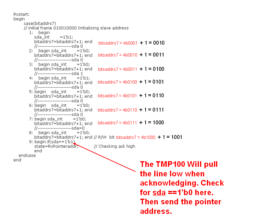
This thread has been locked.

If you have a related question, please click the "Ask a related question" button in the top right corner. The newly created question will be automatically linked to this question.

TMP 100 Evaluation board

Other Parts Discussed in Thread: TMP100

Dear All,

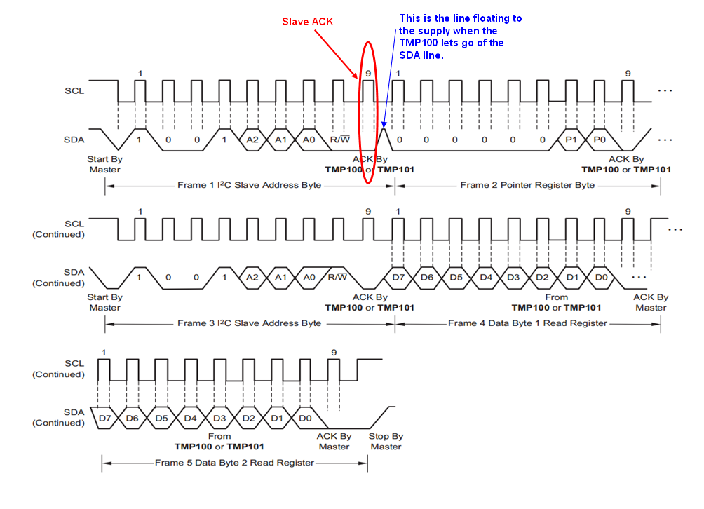
I have a TMP 100 'Evaluation board' and its corresponding PC suite. But I need to connect it to SPARTAN 3E board, so how can I do that ??

while implementing I2C  which device is master? and TMP 100 Evaluation board  outputs data via RS232 so which are the pin numbers ?

And one more thing is .... the data sheet says if we use more data bits like 10,11,12  we will get more accuracy... so in I2C can we simply put this  data bits?? 

  • Hi Fradaric,

    The TMP100 would be an I2C slave.  It looks like you could pick off SCL and SDA from test points one and two (respective) back to your FPGA board.  The TMP100 is actually supported through our Temp Sensor forum, so I'll move your post there and perhaps get you a more complete answer/solution to your problem.

  • Fradaric,

    1) As seen in the schematic below you can connect to SDA through test point TP2 and SCL through test point TP1.

     2) While implementing I2C communication using the TMP100 the master will be the micro controller or FPGA. The TMP100 is the slave. 

    3) By default the TMP100 will provide 9 bits of resolution. You are able to change the resolution to 9, 10, 11, or 12 bits. This is done by setting bits R1 and R0 in the configuration register to the desired resolution as seen in Table 8 below. The most significant bits in the temperature register are used with the unused LSBs set to zero.

  • Since I am using TMP100 Evaluation board, how can I power up the device. I don't wanna coonect it to a PC via RS232.

  • Fradaric,

    As seen in the schematic above you can hook up a separate power supply to J1 pin 1. The TMP100 can operate at a supply range from 2.7 to 5.5V. The most common voltage to power on this device is with 3.3 V.

  • I need continuous temperature values, so In my design I put  '1001000' after the start bit and again '0' as R/W then waited for ack an then  '000000-00(P1P0) like that. Is it the right procedure?  

    Verilog code with in-out pin is difficult to check via test bench, so I need someone to verify my design.

    Here is my code

    ////////////////////////////////////////////////////////////////////////////////////////////////////////////////////////////////////////////////////////////////////////////////////////////////////////////////////////////////////////////////////

    `timescale 1ns / 1ps
    // Fradaric Joseph
    // Indian Institute of Technology Guwahati
    // Ph: 09401015142

    module I2C(
        inout sda,
        output scl,
        output [15:0] temperature_out,
        input clk
        );

    parameter clock_div=500; //  I2C clock 50MHz/(500)=100KHz
    //---------------------------I2C State Machine Variables----------------------
    parameter Rxidle    =0;
    parameter Rxstart    =1;
    parameter RxPointeraddr    =2;
    parameter Rxdata    =3;
    parameter Rxstop    =4;
    //-----------------------------------------------------------------------------
    reg chk=0;
    reg ack=0;
    reg ack1=0;
    reg ack2=0;
    reg ack3=0;
    //------------------------------------------------------------------------------
    reg I2Cclk            =0;  // I2C clock
    reg [8:0] clkclk=clock_div; // in order to divide 50MHz clock
    reg sda_int            =1; // making SDA high in initial state
    reg [15:0] outreg    =0;
    reg [3:0] I2C_counter=0;  // for giving the pointer address (000000-00(P1P0))
    reg [3:0] bitaddrs7=4'b0001; // initializing via giving slave address(1001000-0(R/W))
    reg [3:0] Rxcount=0;// receiving data from TMP 100
    /// ----------------------------------------------------------------------------
        reg [2:0] state     =Rxidle ; // For State machine starting
        assign sda    =sda_int; // Using SDA pin
        assign scl    =I2Cclk;// Generated Clock for I2C
        assign  temperature_out = outreg;  // output from TMP 100
    ////------------------------------
    always @ (posedge clk) /// --------------------- scl generation-----------------
    begin
        clkclk=clkclk - 1;
    if(clkclk==0)
        begin
        I2Cclk=~I2Cclk;
        clkclk        =clock_div;
        end
    end
    ////.............................................................................
    always @(posedge I2Cclk)
    begin
        ////....................................state machine.........................
    case (state)
    //-------------------------------------------------------------------------------
    Rxidle:
                    begin sda_int        =1'b0;    //---------------------start sda = 0
                    state            =Rxstart;end
    //-------------------------------------------------------------------------------                
    Rxstart:
    begin
            case(bitaddrs7)
            // initial frame 010010000 Initializing slave address
                1:    begin
                    sda_int        =1'b1;
                    bitaddrs7=bitaddrs7+1; end
                    //---------------------sda 0
                2:    begin sda_int        =1'b0;
                    bitaddrs7=bitaddrs7+1; end
                    //---------------------sda 0
                3:    begin sda_int        =1'b0;
                    bitaddrs7=bitaddrs7+1; end
                    //---------------------sda 1
                4:    begin sda_int        =1'b1;
                    bitaddrs7=bitaddrs7+1; end
                    //---------------------sda 0
                5: begin    sda_int        =1'b0;
                    bitaddrs7=bitaddrs7+1; end
                    //---------------------sda 0
                6: begin    sda_int        =1'b0;
                    bitaddrs7=bitaddrs7+1; end
                    //---------------------sda 0
                7: begin sda_int        =1'b0;    
                    bitaddrs7=bitaddrs7+1; end
                    //---------------------sda=0
                8:    begin sda_int        =1'b0;
                    bitaddrs7=bitaddrs7+1; end // R/W  bit
                9: begin if(sda==1'b1)
                    state=RxPointeraddr;            // Checking ack high
                    end
        endcase
    end
    //---------------------------------------------------------------------------------        
    RxPointeraddr:
        // Pointer Address 000000-00(P1P0) for temperature register
    begin
            case(I2C_counter)
                            //---------------------sda = 0
                0: begin    sda_int        =1'b0;
                    I2C_counter=I2C_counter+1;end
                            //---------------------sda = 0
                1:    begin sda_int        =1'b0;
                    I2C_counter=I2C_counter+1;end
                            //---------------------sda = 0
                2:    begin sda_int        =1'b0;
                    I2C_counter=I2C_counter+1; end
                            //---------------------sda = 0
                3:    begin sda_int        =1'b0;
                    I2C_counter=I2C_counter+1; end
                            //---------------------sda = 0
                4: begin    sda_int        =1'b0;
                    I2C_counter=I2C_counter+1;end
                            //---------------------sda = 0
                5:    begin sda_int        =1'b0;
                    I2C_counter=I2C_counter+1;end
                            //---------------------sda = 0
                6:    begin sda_int        =1'b0;
                    I2C_counter=I2C_counter+1;end
                            //---------------------sda = 0
                7:    begin sda_int        =1'b0;  
                    I2C_counter=I2C_counter+1;end
                8:    begin    if(sda==1'b0)
                    state=Rxdata;      ack1=0;end // after pointer register sda line acknoledged by a low    pulse    
                endcase
    end
    //----------------------------------Receiving Temperature Data --------------------------
    Rxdata:
    begin
        case(Rxcount)
            0: begin outreg[15]=sda;
                Rxcount=Rxcount+1;end
            1: begin outreg[14]=sda;
                Rxcount=Rxcount+1;end
            2: begin outreg[13]=sda;
                Rxcount=Rxcount+1;end
            3: begin outreg[12]=sda;
                Rxcount=Rxcount+1;end
            4: begin outreg[11]=sda;
                Rxcount=Rxcount+1;end
            5: begin outreg[10]=sda;
                Rxcount=Rxcount+1;end
            6: begin outreg[9]=sda;
                Rxcount=Rxcount+1;end
            7: begin outreg[8]=sda;
                Rxcount=Rxcount+1;end
                                            // low pulse acknoledgment from TMP100
            
            8: begin outreg[7]=sda;
                if(!sda) ack2=1;
                Rxcount=Rxcount+1;end
            9: begin outreg[6]=sda ;
                Rxcount=Rxcount+1;end
            10: begin outreg[5]=sda ;
                Rxcount=Rxcount+1;end
            11: begin outreg[4]=sda;
                Rxcount=Rxcount+1;end
            12: begin outreg[3]=sda;
                Rxcount=Rxcount+1;end
            13: begin outreg[2]=sda;
                Rxcount=Rxcount+1;end
            14: begin outreg[1]=sda;
                Rxcount=Rxcount+1;end
            15: begin outreg[0]=sda;
                    if(sda==1'b0) begin ack3=1; // checking low pulse acknoledge frm TMP 100
                        state=Rxstop; end end
            endcase
    end
    //-----------------------------------------------------------------------------------------
    Rxstop:
    begin sda_int=1'b1;end  
    endcase
    end
    endmodule

    ///////////////////////////////////////////////////////////////////////////////////////////////////////////////////////////////////////////////////////////////////////////////////////////////////////////////////////////////////////////////////

  • Fradaric,

    I looked through your code and found the following error. It looks like you are checking for the TMP100 to ack high. The TMP100 will pull SDA low when it acknowledges. Try changing this and then send the pointer address when the TMP100 pulls the line low. I attached the timing diagram for convienence below. Please see the 9th bit. We can step through debugging this together after this change is made. Also I would recommend using an oscilloscope on SDA and SCL while you are debugging. It will help to see what is being sent out on the communication lines.

  • Yehh,   I made the changes and also I found its operating frequency is 50KHz.. Can I go further? my Timing diagram shows its fine.  Just tell me any other mistakes in my code..   

    Thanks

    Fradaric

  • Hi, I am waiting for your opinion

    Fradaric

  • Hi, I would appreciate if you can give me a verilog interface(I2C for TMP100), if you have one. I don' t have enough time left in my project.

  • Fradaric,

    I have looked around online and have found this resource for you.Please see the link below. At the bottom of this link there is a verilog file and screen shot showing what the timing should look like. This is not specific to the TMP100 but should give plenty of guidance on how to approach the communication using verilog.

    http://www.fpga4fun.com/I2C_2.html

  • Yes, I found the code. But I would like to know about my design too. Can I proceed with the code I've shown you? is there anything wrong you feel, and what about configuration register settings? 

  • Fradaric,

    I do not see in your code where the last 3 bits of the slave (TMP100) address comes from. Specifically the address should be a 7-bit address that is either 

    1001000, 1001001, 1001010

    As I pointed out above you have indicated the first 4 bits 1001 and check for a slave acknowledgement. I do not see 1001 followed by the rest of the address. The edges of SDA also appear to coincide with the clock edges of SCL which is not valid in I2C. There is a setup time requirement that must be met with I2C. Specifically this is a 100ns setup time that can be seen on page 10 of the data sheet. 

  • case(bitaddrs7)
            // initial frame 1001000 Initializing slave address
                1:    begin
                    sda_int                =1'b1;     //---------------------sda 1
                    bitaddrs7=bitaddrs7+1; end
                    
                2:    begin sda_int        =1'b0;//---------------------sda 0
                    bitaddrs7=bitaddrs7+1; end
                    
                3:    begin sda_int        =1'b0;//---------------------sda 0
                    bitaddrs7=bitaddrs7+1; end
                    
                4:    begin sda_int        =1'b1;//---------------------sda 1
                    bitaddrs7=bitaddrs7+1; end
                    
                5: begin    sda_int        =1'b0;//---------------------sda 0
                    bitaddrs7=bitaddrs7+1; end
                
                6: begin    sda_int        =1'b0;//---------------------sda 0
                    bitaddrs7=bitaddrs7+1; end
                    
                7: begin sda_int        =1'b0;//---------------------sda=0     
                    bitaddrs7=bitaddrs7+1; end
                    
                8:    begin sda_int        =1'b0;
                    bitaddrs7=bitaddrs7+1; end // R/W  bit
                    
                9: begin if(sda==1'b0)
                    ack=1'b0;
                    state=RxPointeraddr;            // Checking ack high
                    end
        endcase

    I think this is what you talking about! right? the cases 1 to 8 indicates the address 1001000 and the 9th case is R/W and that is zero as per the timing diagram. Then??

  • Please give me a reply if you don't mind!. I was in a hurry and the example you have given me is not applicable  for me since it is a slave. I hope its better go for my own design rather than editing someones code.  I put the delay you have mentioned directly in to the code like #100;  sda_int =1'b0; .

    I would be grateful to you if you could give me a solution.

    Thanks,

    Fradaric

  • Let me know the values in  P1 and P0, In order to get  data output from TMP100. (I am putting '00' now)

    And I am confused with adding setup time into my design.  Someone please help me..... how to include  setup time?? 

    Also I would like to know the configuration register settings, Is it included In the timing diagram? I need a resolution of 12 bits, how can I do that?

  • P1 and P0 form the pointer.  The pointer tells which register you will read or write to.  There are four different registers in the TMP100.  The pointer will determine which of the four registers that you read or write to.  Table 2 on page 5 of the data sheet tells the value of P1 and P0 required to write or read each of the registers.  For example, if P1/P0 = 00 you will read from the Temperature register.  If P1/P0 = 01 you can read or write to the configuration register.

    To change the resolution to 12 bits you need to write to the configuration register.  Table 6 shows the format of the configuration register.  Bits 5 and 6 set the resolution.  These bits both need to be high.  Of course you must write all the bits of the configuration register, so when you set the resolution you will also change other configurations.  You will need to determine what you need all the other bits in the register to be.  If you don’t want the part shut down and you don’t care about the alert status the configuration below should work.

     0110 0000 == sets resolution to 12 bits, continuous conversion

     I am available for a call tomorrow.  Email your phone number if you want to discuss this on the phone.

     Art Kay

    Email: Kay_art@ti.com

  • Fradaric,

    Please see table 1 and table 2 in the product datasheet on page 5. The pointer register is an 8-bit register. Bits P0 and P1 are the least significant bits within this register. These bits are used to address the other four registers in the TMP100. With P1 = 0 and P0 = 0 you are talking to the temperature register as seen in Table 2. 

    If you would like to configure the device to 12-bits of resolution you will need to address the Configuration register (P1 = 0 and P0 = 1) and perform a write operation as seen in Figure 6. Setting bits R1 = 1 and R0 = 1 in the configuration register will configure the device to provide 12 bits of resolution.

    For each clock pulse the data you are sending needs to be setup or valid before a rising clock edge. In other words if you want to send a 1 than that 1 needs to be setup at least 100ns before the next rising clock edge. Please refer to Figure 5 in the datasheet. Specifically see tSUDAT in this figure for a visual description. 

  • Chris Featherstone,

    somehow I finish coding...thanks a lot, you guys really helped me... And I   got sample TMP100NA/250 from TI, the chip seems too tiny, any specific PCB's available for that, or interconnecting slots?.

    I may face problems when doing real hardware interfacing rather than test-bench, hope u will be there for me till  I read temperature from TMP100.