This thread has been locked.

If you have a related question, please click the "Ask a related question" button in the top right corner. The newly created question will be automatically linked to this question.

tmp006 pcb design insights

Other Parts Discussed in Thread: TMP006

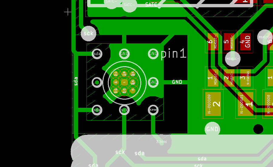
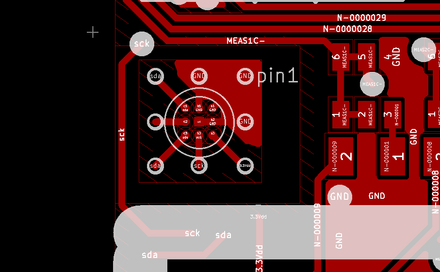
Hi, we recently design a pcb with the tmp006 installed.  We followed the guidelines for installing tmp006 into a pcb (or so we believe see below for details).  We have good communication (no problems with I2C), but the signal is going in the opposite direction that it should (hotter shows colder, and vice versa) and is very wobbly.  The die temperature seems to be showing correctly, the problem is only with the IR calculated temperature.  We also have an Adafruit TMP006 module which works without any problems - so we know what 'working' looks like.  The difference between our PCB design and theirs are minor, and we can't quite figure out why our signal is so much worse.  See the images below for a description of the top and bottom of the pcb the tmp006 is installed on.


We recently removed the tmp006 chip from the the Adafruit board and installed a new tmp006, just to see if the problem is that we are doing a poor job soldering the unit - but the results still looked very good using our solder job.  So we are pretty sure at this point it's a difference in the design of the pcb.

Note - We know that c2 (DRDY) pin should be pulled up - we had installed a 10k resistor since.  Also, we've added an additional .1nF cap closeby, but that didn't seem to help either.  Also, (in case you're wondering) the I2C address 0x42 (ADR1 - GND and ADR0 - SDA).

The size of the ground planes separating the tmp006 from the rest of the pcb is: the inner ground plane is 4.5 x 4.5, while the outer ground plane is 6.8 x 5.8mm.  When a temperature measurement is being taken, none of the nearby traces oscillate.  We are using an arduino and Adafruit's example TMP006 sketch for testing.  We do not have any components nearby generating IR signal which could cause interference.

Any ideas based on looking at the layout on what our problem might be, or any other suggestions?


Thanks,

Greg

top of PCB:

bottom of PCB:

  • Hello Greg,

    Thanks for the detailed post, its really helps understand your issue. Unfortunately, I'm unable see to any pictures attached along with the post as per your description. Can you please re-attach the images?

    Thanks,

    Abhi

  • Shoot - sorry about that, I could see them in the wysiwyg editor --


    bottom:

    top:

  • Hello Gary,

    A quick check: I2C address is 0x84 for Write (ADR1 - GND and ADR0 - SDA) and 0x85 for Read. Its not 0x42 as you mentioned. Can you please make sure you do not have the wrong addres.

    Regards,

    Abhi


  • The address for the device is (based on page 7 here - http://www.ti.com/lit/ds/symlink/tmp006.pdf) 1000010 which is 0x42.  I suppose then you have to add a read or write bit as well.

    Am I mistaken here?  I'm using the adafruit library (in C++) which simplifies things a bit, but given that it works well for the same exactly setup on adafruit's tmp006 breakout (and that you do get a response from having objects in front the tmp006 though that response is backwards), I'm guessing that the read and write commands are working ok -


    Greg

  • My thought (i'm Greg's coworker that is doing the ee design).

    We ordered solder coated prototype board from advanced circuits (24 hours turnaround time barebones with no soldermask or silkscreen) with ultra low emissivity on copper surfaces (it acts like a IR mirror, since i use infrared camera i can confirm that with image) .

    It is more important issue then "thermal time constant" of the PCB underneath the chip that you mention in the datasheet, matched emissivity to the most common material, since you have another termopile facing bottom of the chip, for reference comparison, counting on board temperature you measure in the chip and fixed emissivity which you probably optimized for most common (green soldermask).

    It should be mentioned in the datasheet since the effect is severe (going as high as reading high negative temperatures because of ref termopile temperature reading is way off due to the emissivity mismatch)

    We will test the idea with paint (hard to apply in the middle of the BGA9 footprint) but count to solve that issue with proper soldermask and maybe even add some black silkscreen dot beneath the chip, (using flir I7 i can skew temperature reading on green soldermask by few c using my IR hand signature as a reflection) ...

    Regards

    Robert Zegarac

  • Verified, Coating copper fill under the TMP006 with high emissivity paint solves the problem.

  • Robert & Gary,

    Thanks to both of you for posting and following up with your status. I'm glad that you were able to solve the issue by making the copper fill more emissive/less reflective.

    When you initially mentioned that "signal is going in the opposite direction that it should (hotter shows colder, and vice versa) and is very wobbly" I'm assuming what you see is noise induced in the signal (not an offset effect). I'm guessing this is noise caused do to the light incident on the reflective surface of the copper fill at the lower surface of the thermopile. This is the only possible logical explanation I can make out of it because we did compare the cooper fill with and without the solder mask and they made no difference in terms of the offset. 

    Thanks for pointing out this effect. I will make sure our systems engineer is aware of this phenomenon and we will make sure that this gets mentioned in the data sheet and application guides.

    Best Regards,

    Abhi