This thread has been locked.

If you have a related question, please click the "Ask a related question" button in the top right corner. The newly created question will be automatically linked to this question.

LDC1000's ODR

Other Parts Discussed in Thread: LDC1101

Hello TI Team!

On page 5 of the LDC1000's datasheet (electrical characteristics) the min. and max response times of the sensor are given with (Responsetime x 1/f_sensor).

On page 21 the sensor's ODR is calculated using Responsetime/3.

What is the difference between min/max responsetime and ODR?

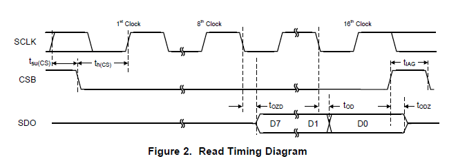
On page 7 (timing requirements) what is the t_IAG (Inter Access-Gap) or where can I find it in the diagram?

Thank you,

Regards, Thomas

  • Hello Thomas,

    The conversion interval is RESPONSE_TIME / (3 * fsensor), which is the ODR (output data rate). Response time is related to the impulse response time; it is effectively a device configuration which sets the conversion interval.

    The t_IAG is the minimum time that CSB must be held high before a new SPI transaction.

    Regards,

    ChrisO

  • Thank you for your fast reply ChrisO!

    Your answer leads me to my next question:

    With fastest possible ODR (12,8µs) and 48bit to read, it'll need about 266ns per bit.

    So data read is already pritty close to the maximum f_SCLK of 250ns (4MHz).

    Is it actually possible to deliver every measured value?

  • Hello Thomas,


    Yes, it is fast enough to retrieve all of the data; you are correct in that it is rather tight timing. If you are using a sensor with 5+MHz, you may consider looking at the LDC1101, which is a faster part - it can go up to 10MHz for the sensor, and has an 8MHz SPI bus.

    Regards,

    ChrisO