This thread has been locked.

If you have a related question, please click the "Ask a related question" button in the top right corner. The newly created question will be automatically linked to this question.

PGA900 4-20mA output mode

Other Parts Discussed in Thread: PGA900, USB2ANY

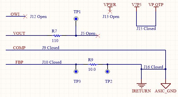
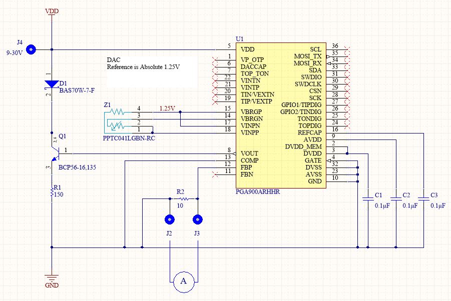
I have a simple sensor that I'd like to connect to the PGA900 and get a 4-20mA output.  The image below shows the a schematic of the sensor.  

I'm a little confused on what pins I should be connecting this sensor to.  I have the PGA900 setup as described on page 119 of SLDS209A. 

Any help or guidance would be greatly appreciated.
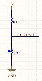
Thank you,

  • Hi Kevin, the PGA900 pressure input pins are differential (VINPP and VINPN). Based on your schematic, I am assuming this is only one of the legs of the sensor (VINPP for example) and the second leg (VINPN) would be connected to a fixed voltage. The PGA900EVM offers something similar to this setup where VINPN is connected to a fixed voltage of about 1.25V (assuming VBRGP=2.5V) and VINPP is changed by having a digital potentiometer in that leg. Please refer to the EVM schematics in p.16 of the EVM user's guide, the document number is SLDU011.

    In addition, please notice the pressure input common mode constraints for the PGA900 shown in p. 11 of the datasheet. As you can see, the single-ended voltage for either VINPP and VINPN should be between 0.3 and 1.8V. Therefore, using a 5V supply for your sensor will probably not satisfy this. Usually, the sensors are excited by the device itself (PGA900) using VBRGP and VBRGN. If you configure VBRGP to 2.5V and following my recommendations above for the legs of the sensor, then you should be good satisfying the common-mode range constraints.

    Please also notice that in order for the PGA900 to operate in 4-20mA loop (or any other output mode) will need firmware in the M0. You can find a reference firmware and use it as a starting point in the product folder. The file is called "PGA900 Generic Firmware". You will need Code Composer Studio (CCS) to compile the firmware and the PGA900GUI (available also at the product folder) to download it to the device. There are also quick start guides for the reference firmware and GUI available at the product folder.

    Let me know if you have any other questions, thanks,

    JV

  • Hello JV,

    Your input is getting me closer to my goal.  However I do have some confusion about the jumpers since the diagram from p.16 of SLDU011 shows one way to setup jumpers for 4-20mA output and table 2 on p.7 of SLDU011 show another way.  There are some contradictions there.  

    Also,  I had the idea I can use the GUI to make the needed changes to the registers as outlined on p.119 of SLDS209A and with it setup that way I would be able to adjust DAC REG0 and monitor the 4-20mA output between TP45 and TP42. Are you saying I still need the generic firmware loaded before that is performed too?

  • Hi Kevin, the jumper configuration comments in p. 16 of SLDU011 is based on a previous revision of the EVM, it's a typo and I will fix it. Table 2 on p. 7 of SLDU011 is correct.

    Now, if all you want is to write to the DAC and measure the loop current, you are correct, you don't need generic firmware for that and you can just follow the steps in p. 119 of SLDS209A. Please notice that, due to the same typo you mentioned, you should use TP3 and TP2 to measure the loop current (not TP45 and TP42). Just make sure you measure R9 before to accurately convert the voltage to current.

    The firmware is needed to relate the inputs to the PGA900 to the output of the PGA900 (loop current in your case), that is, the PGA900 output will respond to changes in its input. However, you can just write to the output directly as I mentioned without the need for firmware.

    Thanks,

    JV

  • JV,

    I'm not getting the response I'm expecting from the PGA900 and I know it has to do with jumper settings.  I created a schematic (below) showing the jumper setting configuration called out by "DAC OUTPUT CONFIGURATIONS" in SLDU011 p.16.  Also, J1 shows (pins 1-2)? 

    R9 reads 9.78ohm on my bench top DMM.

    For now I think I'd be happy having the PGA900EVM running a testable current loop controlled through DAC_REG0. But I'm not there yet. Can you provide a table or image of the EVM with the jumper setup for a 4-20mA loop test?

  • Kevin, as you suspected, your jumper settings are not correct. For 4-20mA operation, the output stage must be configured the following way:
    1. Close J4, J5, J9 and J10.
    2. Open J6, J7 and J8.

    Unless you are programming the OTP in the device, J15 should be open. J15 should be closed ONLY when you are programming OTP. In addition:
    1. J16 must be open for 4-20mA operation.
    2. J19 must be set depending on whether you are using I2C/SPI or OWI. However, since this device will not have firmware based on what you have mentioned, then it will have to be I2C or SPI so set J19 to pins 1-2.
    3. J14 should be set to pins 1-2.
    3. Open J11 and J12 and close J13 (same voltage applied to the EVM will be the voltage applied to PGA900).
    4. Assuming you use SPI, open J25, J27 and close J24, J26, J28 and J30.

    After this, you should be ready to set the registers to 4-20mA configuration using SPI.

    Thanks,

    JV
  • JV,

    Your last update enabled me to use the EVM to get a 4-20mA output and by adjusting DAC_REG0 that output could be adjusted.  Thank you for help on that!

    For any readers of this post, note when using the EVM GUI to update your EVM you must apply power to the EVM J20 and 21, prior to using the GUI. I made the mistake thinking I would be able to do all the register adjustments I needed with just the USB supplied power.

    I've been playing around with my sensor and trying to adjust the EVM so that I can use the sensor "Z1" as drawn in the schematic below. I have bypassed the external bridge by removing J1, J2 and J3 from the EVM.   VBRDG_CTRL is set for a 1.25V output which I plan to use as you can see below.  The sensor basically will divide the voltage which I expect to read on VINPP. 

    My question is; should I be able to configure the EVM using the GUI to accomplish my 4-20mA output without having to write a custom program?  Please let me know if you need any more detail.

  • Hi Kevin, I am glad you got to work the 4-20mA loop operation. Regarding your test with your sensor, yes, you will need firmware in the PGA900 to relate the input to the PGA900 to the output of the PGA900. This is because the PGA900 is an open core device and, as a result, the analog front end needs to be linked to the analog output using digital firmware. This is shown in the figure below. However, you can use the reference firmware at ti.com as a starting point. The reference firmware is located at http://www.ti.com/lit/zip/sldc010

    In addition, looking at your schematic, there is a mistake regarding the FBP pin. FBP is the return path for the loop current back to the controller. In other words, the other end of R2 cannot be connected to GND of the PGA900. It should be the connection to the negative terminal of the controller. There is an app note that describes the operation of the PGA900 as a 4-20mA loop transmitter. Please take a look at Fig. 1 and you will see the issue with FBP that I am talking about.

    http://www.ti.com/lit/an/slda030/slda030.pdf

    Finally, you will need to be careful with the common-mode requirements for the PGAIN inputs and outputs. The single-ended voltage for the PGAIN input must be between 0.3V and 1.8V and the single-ended voltage for the PGAIN output must be between 0.1 and 2V which means you need to select a value for PGAIN to fit this requirement.

    Thanks,

    JV

  • Hi Javier,

    I'm now working on the programming end with our programming engineer. We are struggling to load anything we can verify. You have documents and guides but how useful are they if the end result is confusion and not knowing how if they are accurate? The current limited examples and guides makes using this IC a challenge. Can you provide a contact number so that we can conference call in and talk in more detail and make some progress on our end?

    -Kevin

    Here is Daniel our Programming Engineer's comments:
    =======================================================
    Hi Javier,

    We've tried quite a few things, but I simply cannot verify that a program is a) being compiled correctly, and b) that the .hex binary is being executed by the ARM Cortex A0.

    Setting up the compiler/CCS 6:
    I followed all the instructions in the PGA900 Software Quick Start Guide.pdf document that came with the PGA900 Generic Firmware (Rev A) zip file. The compiler setup instructions were written for Code Composer Studio 5, but I am familiar with Eclipse and was able to set up the library paths and Intel Hex conversion tool to be able to build the example firmware and correctly generate a .hex file for download with the PGA900 GUI Tool. We are using the tool with a USB2ANY adapter, so we are limited to using the PGA900 GUI software to download our hex file. In CCS 6, I resolved all build errors and warnings by setting up the library paths and other options. I did not modify any source code.

    Downloading a .hex file into DEVRAM:
    I followed all the instructions I could find on the net, including your posts to other customers like this one:
    e2e.ti.com/.../437433

    We were able to use the PGA900 GUI tool to:
    1. hold the micro in reset
    2. cleared the REMAP register (bit 0)
    3. download the .hex file with the tool
    4. set the REMAP register bit (bit 0)
    5. release the micro from reset

    At the point of releasing from reset, I would expect to see the program executing. To reduce complexity and rule out register configuration problems, I tried executing the most basic program I could come up with - a simple GPIO toggle. Afterall, if the CPU is awake enough to set configuration registers, it should be able to toggle IO pin registers. Here is the source code of my main:

    void main(void)
    {

    GPIO_DIR = 0x00; //set gpio direction register to be outputs

    while(1)
    {
    GPIO_OUTPUT ^= 0x03; //toggle bit 0 and bit 1
    }

    }

    Running this code, I don't see any change in IO pin state. I also am monitoring current consumption by the PGA900EVM board, with 100 uA precision. I see no change in current consumption when the microcontroller is released from reset. To me, this indicates that the CPU never really begins executing instructions.

    Do you have any suggestions?

    Thank you,
    Daniel
  • Hi Kevin and Daniel, I notice you are using CCSv6, by coincidence, we just finished updating the software quick start guide based on v6, it's just not online yet. I will send you an e-mail with this preliminary user guide to make sure we are not facing a CCS version conflict resulting in a wrong .hex file. I will also send you the .hex file that the reference firmware generates just for quick verification.

    Also, please notice that while the microcontroller is running, only the following registers can be read using the PGA900GUI:

    1. MICRO_INTERFACE_CONTROL
    2. COM_MCU_TO_DIF_B1
    3. COM_MCU_TO_DIF_B2

    And only the following register can be written using GUI:-

    1. COM_DIF_TO_MCU_B1
    2. COM_DIF_TO_MCU_B2

    Therefore, one quick way to check whether the micro is in fact running, is to read the MICRO_INTERFACE_CONTROL register using the Low-Level Configuration tab in the PGA900GUI. If the result is 0x03, the micro is in reset and digital interfaces are enabled. If the result is 0x00, then the micro is running.

    I will send you the e-mail now. Thanks,

    JV

  • This issue was resolved after a call with the customer.

    JV