This thread has been locked.

If you have a related question, please click the "Ask a related question" button in the top right corner. The newly created question will be automatically linked to this question.

TMP112 - Address 0x4A does not worl

Other Parts Discussed in Thread: TMP112

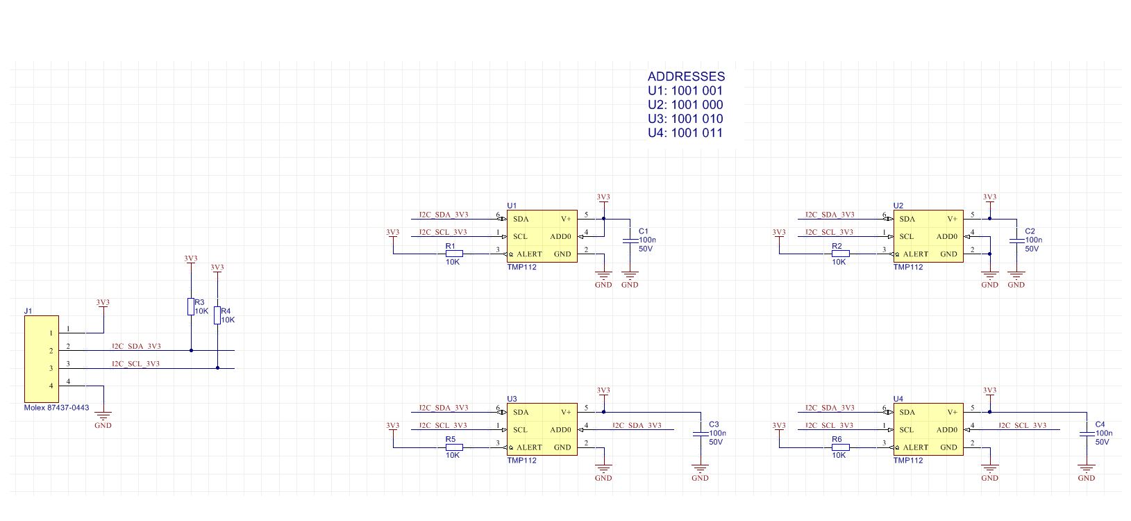
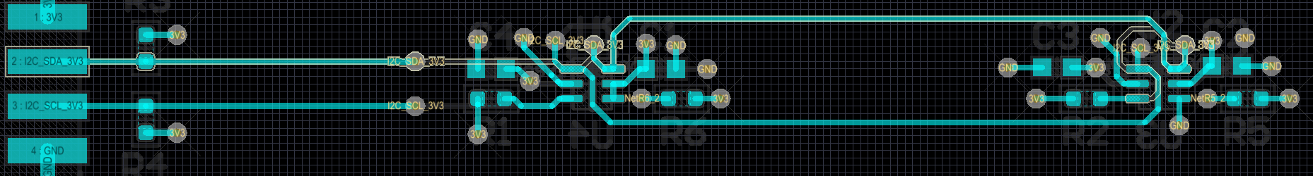
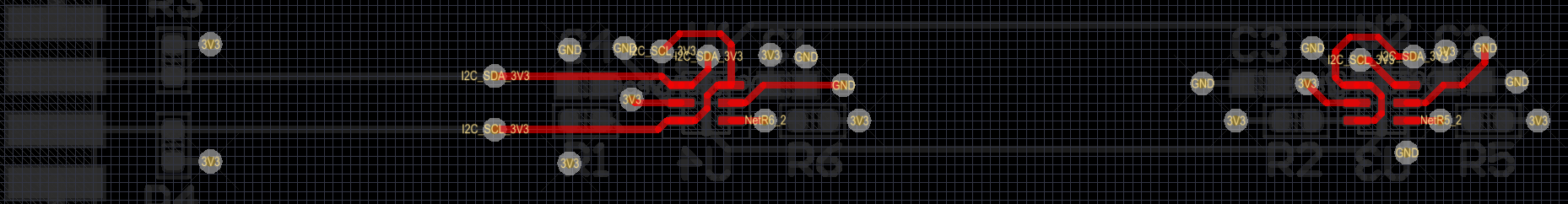
We have a board that essentially just has I2C communications coming into it, that are connected to 4x TMP112. The TMP112 has four possible available addresses, depending on what you connect the ADDR pin to, however it appears as though one of the addresses does not seem to work for us. When the ADDR pin is connected to the SDA line, the device should use I2C address 0x4A, however nothing appears on that address. We have hooked up a scope to verify that the correct waveforms do appear on the SDA and ADDR lines ruling out signal integrity issues.

This is happening across all of the boards we made, and we have tried assigning one of the other chips to this address instead but it still did not appear.

Does anybody has any suggestions?

Best Regards,

Chee Boon

  • Hi Chee Boon,

    The schematic is looking good except that the pull-up value might be a bit too high. We recommended a 5kΩ pull up resistor. Could you please provide a raw file of the scope photo when you tried to communicate to the 0x4A?

    Aaron
  • Hi Chee Boon,

    We validated all the possible addresses in our system, and they are working properly as expected. We believe that there might be a possible of timing limitation issue when the address pin that is tied to SDA signal. The SDA and SCL address options relay on the address pin must be identical communication protocol. We suspected that the routing for the U3 address pin is unusual, it could cause signal skew or jitter relative to SDA. As a result, the device detects an incorrect address. We would like to see the following items below.

    1. Please provide your board layout.

    2. A scope shots of the communication for SDA and SCL if possible address pin.

    Aaron

  • Hi Chee Boon,

    Just checking in with you if you are able to get the scope snapshot and your board layout.

    Aaron
  • Hi Aaron,

    I'm the client of Chee Boon who asked this question, figured it will probably be easier for me to respond directly from here! I have taken some DSO images of the communications lines as seen below. It all looks pretty clean (some overshoot and very minor coupling, but seemingly no delay between SCL / SDA), and the routing is fairly straight forward and short (signal trace lengths ~40mm). I have attached screenshots of the routing also (connector on the left goes to any external I2C host, in the case of the screenshots below it was connected to an Arduino, although it is typically connected to an FPGA).

    In relation to the higher value pullups, we have also attempted to drive this board from another system which has 1k pullups on that line as well, and suffered the same issues, although we may replace the 10k with 5k on one board to test, just to cover all bases.

    In the first image, the read from address 0x4A can be seen to be NACK on the left, while the read from address ox4B on the right is successful.

    Top layer routing -

    Bottom layer routing -

    The device which is not responding is the one on the right on the bottom layer.

    Cheers,

    Oliver

  • Hi Oliver,

    Thank you for the snapshot. I need time to review this, and get back to you.

    Aaron
  • Hi Oliver,

    Can you confirm that the picture with time stamp of 9:02:24 is depicting Data Hold Time (HDDAT)? There is a timing table on page 6, and an illustration on page 14 of the datasheet. Unfortunately, we have a known issue on this product with zero hold time. This is reflected in the 100ns specification on page 6. It is possible, and we are working to confirm, that different address options have a different hold time dependency. This could explain why you only have an issue communicating with address 4A. Either way, the aforementioned scope picture shows a violation of this 100ns spec.

    Ren
  • Hi Ren,

    I can confirm that the picture with time stamp of 9:02:24 is depicting Data Hold Time (HDDAT). From my capture, it appears as though there was a very slight delay, but fairly negligible. That is unfortunate to hear that this problem exists, especially given that it makes this address unusable with fairly standard I2C controllers (such as Arduino). If you manage to recreate this issue on your end and can confirm the existence of this issue within the IC, then that would give me great peace of mind.

    Oliver

  • Thanks for the reply, Oliver. I hope to have a confirmation for you tomorrow, 12/17.

    Ren
  • Hi Oliver,

    I'm following up with you, because I promised I would today. I was able to get some data on hold time today, but I'm learning now that I did it wrong. I will follow up again tomorrow.

    Recently, another user on this forum posted about a hold time problem with an Atmel controller. I've not verified, but he claims to have solved his problem by changing a setting in the controller. That post is here: e2e.ti.com/.../1720030

    You could also try communicating in High Speed Mode. You'll notice that the HDDAT spec that we discussed earlier is lower in High Speed Mode. The minimum clock frequency is the same in both modes, so there should be no harm in using it.

    Ren
  • Hi Oliver,

    We were able to confirm that the Data Hold Time (HDDAT) significantly increases when pin ADD0 is tied to SDA. This explains why you only have an issue with devices configured for this address. In High Speed Mode, the problem is reduced to a point that should be acceptable for your application. High Speed Mode is explained on page 13 of the TMP112 datasheet. If you have questions about High Speed Mode, please don't hesitate to ask.

    Thanks for bringing this issue to our attention, and thanks for your patience.

    Ren