This thread has been locked.

If you have a related question, please click the "Ask a related question" button in the top right corner. The newly created question will be automatically linked to this question.

HDC1080 Layout

Other Parts Discussed in Thread: HDC1080, HDC1050

Dear Sir 

I don't misunderstanding about below describe in datasheet  

is ti mean ,DAP connect a dummy PAD (without connect anything) from TOP layer to Bottom layer ??

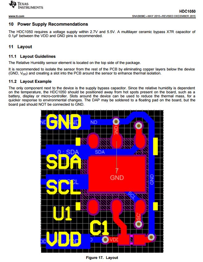
It is recommended to isolate the sensor from the rest of the PCB by eliminating copper layers below the device
(GND, VDD) and creating a slot into the PCB around the sensor to enhance thermal isolation

  • Hi Kai,

    The datasheet suggests to connect the DAP pin to a dummy pad that is not connected to any signal. The dummy pad have to be placed on the top layer OR to the bottom layer, according to the device position on the board. Please refer to the attached layout example:

    In the datasheet it is also suggested to remove any ground plane (or copper layers in general) under the HDC1080, in order to avoid heat conduction from other devices on the board.

    Moreover, to increase the isolation of the device, it is also suggested to cut a little the PCB around the sensor in order to create a socket for the HDC1080 and enhance the thermal isolation:
    Please let me know if this solves your doubts.
    Best regards,
    Carmine
  • Although we would like a land pattern diagram of the HDC1080
  • Although we would like a land pattern diagram of the HDC1080

  • Hi Kai,
    you can find the recommended land patter for the HDC1080 at the following link:

    www.ti.com/.../MPDS498B

    Please, let me know if this reply to your question
    Best regards,
    Carmine
  • Hi Carmine,

    Our layout designer mistakenly connected the DAP pad to ground on the board. This is a prototype board and we will remove the ground connection on the next rev.

    My question is, will the HDC1050 work with the DAP pad connected to ground?

    If so, what are the possible side effects?

    I also want to mention that the HDC1050 layout guidelines are misleading. The DAP pad clearly says GND on it and shows a connection with one of the pads. I think that it would be a good idea to change this drawing. The HDC1080 drawing is more clear.

    Thanks,

    Bob

  • Hi Watanabe

    Attached the recommended land patter for HDC1080:

    2577.1423.HDC1080_recommended_land_pattern.pdf


    Best regards,

    Carmine

  • Hi Bob,
    From the electric point of view, the HDC1050 works correctly also with the DAP pad connected to ground.
    The side effect is that the temperature sensor accuracy could be affected by the heat conduction from other devices on the board.
    The impact of this side effect strongly depends on the configuration of your board: if there are elements which dissipate a lot of power or heat, how far are these elements from the HDC, how is the PCB layout of your board (for example if there is a big ground plane). Unfortunately the temperature accuracy affects also the humidity accuracy: in fact in first approximation for each degree C of temperature error corresponds an error in humidity of about 5% of the actual value. For example if the environmental conditions are 25°C and 40%RH, but the temperature reads from the HDC is 26°C (due to the PCB heat conductions), the value of RH reads from HDC1050 will be 40% * (1-0.05) = 40% - 2% => 38%.

    Yes, you are right: we will update the layout picture in the HDC1050 datasheet. Thank you very much for your feedback and sorry for the inconvenience.
    Please let us know should you have any doubts or need further information.
    Best regards,
    Carmine