This thread has been locked.

If you have a related question, please click the "Ask a related question" button in the top right corner. The newly created question will be automatically linked to this question.

connect the opt8241 to external HW

Other Parts Discussed in Thread: OPT9221, OPT8241, INA226

Hello i would like to connect this EVM to an FPGA to receive the data measurements and would like to confirm how could be done.

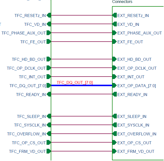
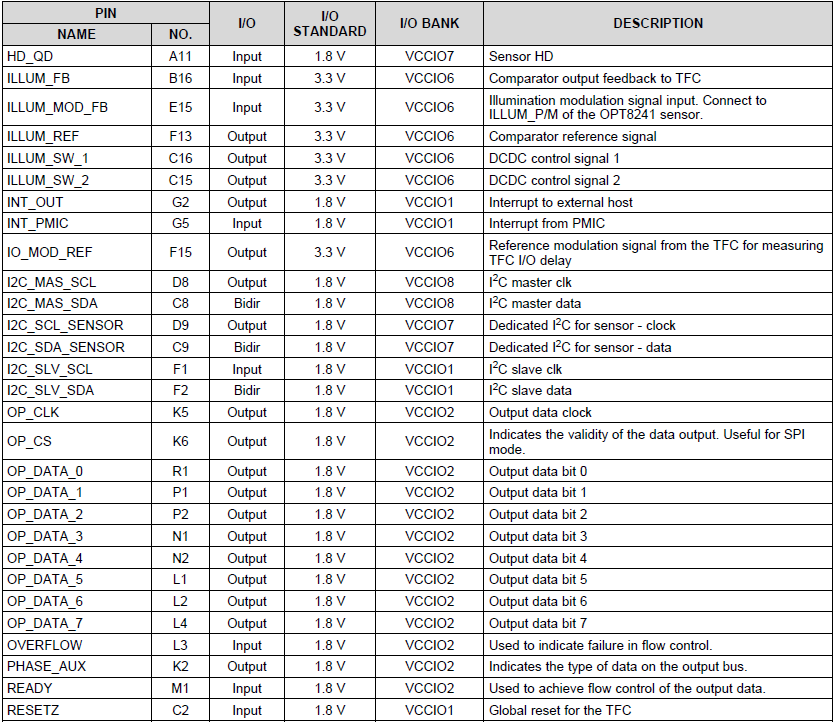
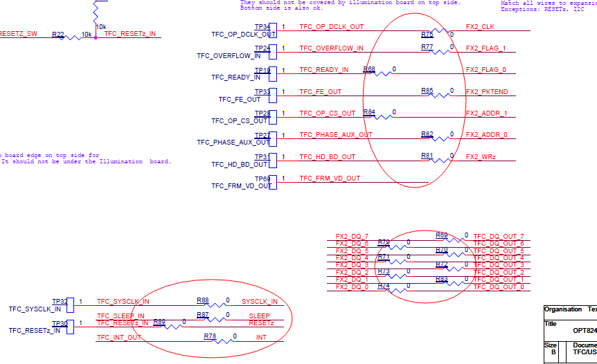
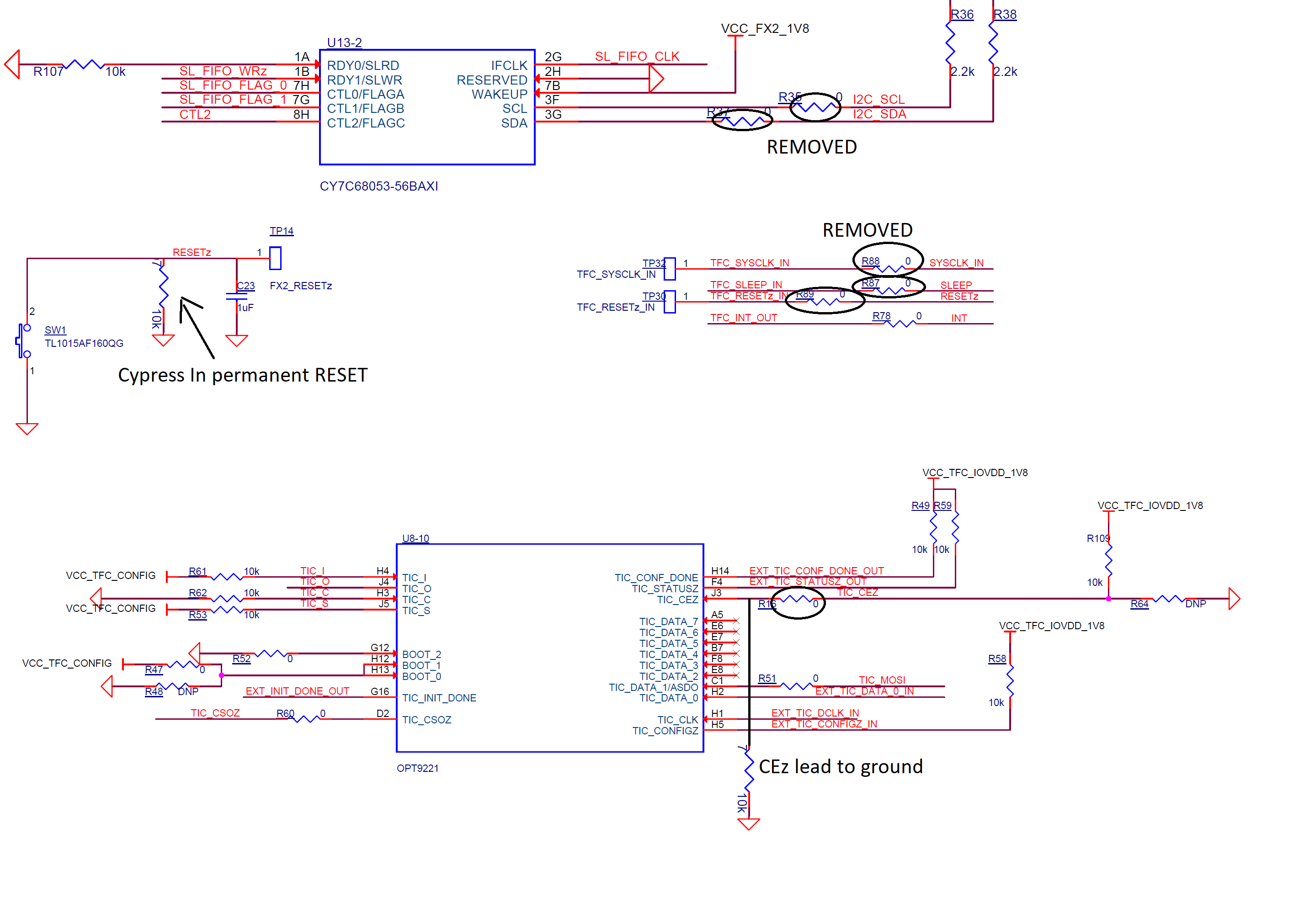
I have seen there is a debug connector (Not mounted) in one side of the EVM and some signals from the OPT9221 are routed to this connector( in schematics the connector is named as ZF5s-40-010T-TW)  but I'm trying to figure out what signals corresponds inside the controller because in datasheet they are named differently.

could you provide more info about this connector and their signals?.

Thanks,

Julian.

  • Hi Julian,

    This is a provision for an expansion connector. The lines going to this connector can enable an external embedded system to take data from the EVM. Please refer to the schematics for the specifics of the actual connections made on the PCB.

    Regards,
    Subhash
  • Thanks for reply,

    I think I have resolve my doubt is about the signals in the connector. In schematics we have:

    And in opt9221 datasheet we have some similar signals:

    Now I have to figure out how interface this connector with a FPGA.

    Thanks.

  • Julian,

    Please let us know if you need any other help. If it is not confidential, can you please tell us something about the application?

    Regards,
    Subhash
  • Hi,

    I am also interested in interfacing the OPT9221 with an external microcontroller using this connector, and I have the following doubts:

    1) In the OPT8241-EVK the OPT9221 is controlled with an FX2, which also interfaces with the PC via USB, is this correct?
    2) With all the lines on this connector, is it possible to control the entire board? It seems to me that the FX2 makes all the settings. I am interested in being able to modify the 9221 internal registers via I2C and then collect the 32-bit data using the 8 data lines.
    3) Do I need to somehow "Power off" the FX2? Or just after the EVK was inicialized I can start interfacing directly with the TFC controller (especially being able to use the I2C lines).
    4) Finally, is there any guide or examples that use this interface?

    Thank you.
  • Hello Cesar and Subhash,

    we also plan interfacing OPT9221 with an embedded system. Our first attempt will be using the 40pin debug connector on the Evalkit to access control and data lines.
    We may exchange experiences here.

    Is there a kind of application note, it would make a good starting point?

    regards,
    Marcus

  • Hi Cesar,

    the FX2 will also work when you connect to external microcontroller .but there is 0ohm Debug resistance for this signal connect to FX2. if you want to use external microcontroller,you shuold take away this Debug resistance. and then connect to external microcontroller.

    Thanks & Regards
    None
  • Hi None

    I have seen in the schematics that in order to use an external microcontroller I should remove R35 and R37 to disconnect the I2C from the FX2 and use mine, but I couldn´t find a resistance to remove that completely shuts down the FX2. Could you tell me which one is this resistance?


    Thanks

    César

  • Hi Cesar

         in the schematics OPT8241-CDK-EVM SB REV2P0V1. all of this resistance should remove form the borad. please see the follow figure.


  • Hi ,

    When you want to connect embedded system to 9221, you have two options.

    1. Control 9221 with FX2. Get only output data to the external system

    You need to connect op data ,op clk signals , TFC_HD _BD_OUT(This is the write enable) to the external microcontroller. Kindly use the op clk for sampling your data.

    2. You want to disable FX2 and use external embedded system to control OPT9221

    The simplest way to disable FX2 is to keep it in reset. If you want to isolate FX2, you can do so by removing the beads B21 and B23 which provides the supply to FX2. Also remove the resistors R35 and R37 to isolate the I2C control signals from FX2. Once FX2 is disabled, you have to provide all the necessary signals and input clock to OPT9221 from your embedded system. All these signals are available on the connector J2. You need not remove every single resistance that is connected to Fx2.

    Regards,
    Nithin
  • Hi Nithin,

    I also want to connect through the debug connector to a System on Chip(SoC).

    In this first step I want to only to acquire the frame data on my SoC. But I do not understand why the signal that have to be connecto to the microcontroller are only op data ,op clk signals , TFC_HD _BD_OUT.

    I saw in the OPT9221 datasheet, ref sect 7.3.4.3.2 8-Lane Mode – Generic Parallel Interface. In this case I need the FE, VD, BD, OP_CLK and OP_Data<7:0>.
     This is the default data transfer to the chip FX2. But I don't found these pin between OPT9221 and FX2, can you help me?

    If I want to get the data with the parallel interface which signal have to be connect to the SoC?

    In this case If I do not connect any USB cable to the FX2 (CY7C68053) I will have the board operative? I mean the signals SLEEP_OUT, INT_IN, TIC_STATUSz, TIC_CONF_DONE, TIC_CONFIGz TIC_CLK and RESETz_OUT

    Thank you

  • Gianluca,

    The OPT8241 and OPT9221 on the EVM are powered by a PMIC which is turned on by the FX2 at startup. The FX2 will boot up as long as it has power, and does not require the USB cable to be connected.

    By default, the OPT9221 boots from EEPROM and should be accessible over I2C automatically. It requires an additional RESETZ which is also asserted by the FX2 at startup.


    The minimum set of signals required for using the 8-lane parallel interface are OP_CLK, OP_DATA<7:0>, BD and either VD or FE. On the FX2, we use the FE instead of the VD signal.

    If you only wish to capture data from the OPT9221 using the debug connector, these signals should be sufficient.
  • Thank you.

    I'm see the signal to the oscilloscope. The follow picture is the TFC_FRM_VD_OUT in DVP and Genreic parallel mode:

    Why you suggest to use the FE signal instead the VD signal?

    The FE signal is on for at least 20ms.

  • The VD is a start of frame marker while the FE is an end of frame marker.

    On the FX2, it is more convenient to use the FE because we can use it to automatically trigger a USB Zero Length Packet (ZLP) or short packet automatically. If we use the VD signal for this purpose, then the ZLP or short packet cannot be sent until the start of the next frame.

    On parallel-to-UVC chips like those from Realtek/other vendors, or DVP hosts, it may be better to use the VD signal.
    The VD signal length and polarity are also programmable as needed.

    You should use whichever signal is convenient for your receiver chip.
  • Thank you for your answer.


    I would like to synchronize the FE signal to the last byte of data. I read in the OPT9221 that it can be possible to set the fe_last_cycle = 0 an have the correct transition. But I didn't have the correct result.

    These are the HD signal and FE signal in DVP mode. When I try to set the fe_last_cycle to 0 or 1 I got the same results.

    In this case If I do the start data syncronization with the FE signal I'll lost the first byte of data. Can you help me?

  • Hi,

    We trying to connect multiple OPT8241-CDK-EVM via the J2 connector, to an own microcontroller based board. Trying to use the onboard FX2 to streaming, and setting via USB but without it's sysclock.

    The following signals are connected to each EVM:

     - All GND pins (1, 7, 12, 17, 22, 25, 30, 37, 40)

    - 13 EXT_FE_OUT (FE) to MCU

    - 16 EXT_SYSCLK_IN (SYSCLK_IN)  - 48MHz clock from a fanout buffer 

    - 36 EXT_VD_IN (VD_IN) from MCU to trigger in slave mode

    The R88 resistor was removed from the OPT8241-CDK-EVM SB, to drive the OPT9221, from external sysclock. The Blue led is glowing after boot.

    If I start Voxel viewer v0.7.0 after the EVM booted up, it works unti I try to change profile, the stream stops and after it gives the next error message:

    ERROR: USBIO: Could not transfer '307200' bytes

    ERROR: USBIO: Could not transfer '0' bytes

    ERROR: USBIO: Could not transfer '0' bytes

    WARNING: USBBulkStreamer: Resetting bulk endpoint at 1479747338794451

    But when voxel viewer is stil running while the EVM booting, and connecting, it gives the same error as above. (as well as Voxel CLI)

    Is there any solutions, or workaround to this problem.

    Best regards,
    Tamas

  • Hi!

    Don't know why, but with 0v26 firmware the camera works better.

    Is there any undocumented new feature, what not mentioned in the changelog?

    Best regards,
    Tamas

  • Hi Tamas

    With 0v26 firmware,the camera works better, I want to know What do you mean better?

    Accuracy or Noise?

    Thanks&Regards.
  • Hi None_feiyu!

    Apparently the noise is a lil'bit less, but the biggest improvement, with the old firmware, all off the cameras booted up 8 out of 10 times, with the new 10 / 10.

    Regards.

    Tamas

  • Hi Tamas

    "all off the cameras booted up 8 out of 10 times, with the new 10 / 10".

    I Can‘t understand what you mean,Could you give me a details description.

    Thanks&Regards.

    None
  • Hi Anand,

    I Have the hardware to connect the opt 8241 to the FPGA. Before connect the OPT to the FPGA I try to see all the OP_DATAs on the oscilloscope I get a problem with OP_DATA_5, see the picture:

    The level is 150 mV and I get this result when I measure OP_DATA_5 on the R70 that is TFC_DQ_OUT_5 ( pag. 9 schematic ) and I got the same results when I measure OP_DATA_5 on the debug connector. At this point I decided to analyze the RAW data frame throught Voxel Viewer, I made this to know if this problem appears on the Cypress side. I set the profile LENS ONLY without any correction and save the phase data. For example this is the first 4 data phase:

    F8 0E      FF 0F     13 0F      89 00

    in bin for the fist value is:

    11111000    00001110

    the bit in bold is the OP_DATA_5

    How it is possible this?

    Could you help me?

  • Hi Nithin


    What I want to do is disable the FX2. I have already removed B21, B23, R35 and R37. From my microcontroller I have been able to read from and write to the PMIC and the INA226 sensors.

    I am fedding the TFC with a 48 MHz clock, already took care of the reset, sleep, ready and tfc_cez pins. (Sleep=0, ready=1, tfc_cez=0). I toggle reset according to the OPT9221.

    According to the BOOT0 / 1 / 2 pins of the OPT9221, the TFC is configured in boot master mode, right? The problem is that I don´t see that the TFC boots. The blue led does not turn on, there is no activity on the output pins and the I2C does not respond. In my circuit I am not using any of the TIC lines of the J2 external connector because I understand that I should control them only when trying to program another firmware for the TFC.

    From what I have understood, the TFC firmware is loaded from the W25Q40BWSN memory. When I check the chip select, miso, miso and clk pins of this memory I see some activity every 100 ms. It stays there like in an infinite loop, like trying to read this memory.

    Could there be something I have forgotten? Or something else that I should do?

    Thanks in advance.

    César Carballido.

  • Hi César,

    Is this still an issue, or did you manage to solve this already?

    - Anand
  • Dear Anand,
    I would like to understand the function of the 128K I2C CMOS Serial EEPROM present in the schematic OPT8241-CDK-EVM SB REV2P0V1 at page 19. Is this the eeprom that has stored the camera hardware profile?

    Regards
  • If you mean U18 on page 9, then this is the EEPROM that contains the firmware for the U13 Cypress FX2 (CY7C68053) chip, and also the calibration profiles.

    Also, please note that U18 should be a 24AA512 (64 kByte) EEPROM. The BOM has the correct part listed, but the Schematic has the smaller 24AA128 - this is a bug and will be corrected in an upcoming schematic update.
  • thank you for your fast reply,
    yes I mean the U18, but in my schematic is in the page 19.
    At this point I have another question: since that the I2C serial eeprom has the camera profile and the firmware for the CY7C68053, the W25Q40BWSN SPI EEPROM has "only" the firmware for the OPT9221?
  • Please make sure you are using the same schematic file as us. Our last released version is available here:
    www.ti.com/.../sbac138

    Yes, the W25Q40 EEPROM has only the firmware for the OPT9221.
  • Thank you for your answer.

    I have another question.

    After connected the opt evaluation board with the FPGA and doing some elaboration, we are now deciding to make a new board which will contains an CU and the two opt: 8241 and 9221.

    Could you have the schematic project file? I mean the DSN file and/or OPJ file. It will be very helpfull for me to have a very good starting point.

    Thanks in advance

    Gianluca

  • Hi Gianluca,

    Could you please take a look at the files in the following link? The DSN files are included in the package for both the illumination (IB) and the sensor (SB) boards.

    www.ti.com/.../sbac138


    Best Regards,
    Anand
  • Thank you, I'm sorry but I was doing the wrong question.
    Is it possible obtain the associated OPJ file?

    Regards
    Gianluca
  • Gianluca,

    The OPJ file is just the project file. We do not normally include the OPJ file in the released schematics and the Orcad tool will anyway create a new OPJ file the first time you open the DSN file.

    May I ask what you expect from the OPJ file?

    Thanks,
    Anand
  • Thanks.
    I was asking you the OPJ file because sometimes my teams send me the two files.
    I'll create the OPJ file from the DSN.

    Thank you
  • Hi Cesar, I have your same problem.

    Now I have disconnected the resistors from 0 ohm of I2C, SLEEP, RESET and SYSCLOCK (R35 R37 R87 R88 R89). At startup I measured the time that the power supply has to have the correct voltage value and it is right (2000 us). Unfortunately, the TFC does not boot. Should I run the reset before booting? Or does the TFC just want the power supplies to be all in t ram time?

    Could anyone help me?

    Thanks in advance.
    Gianluca
  • Gianluca

    What I did with this kit was disconnecting the FX2 and try to control the whole kit with my own micro, using the 40-pin debug connector.

    Here are some tips that could help you:

    - You only have to disconnect the I2C 0 ohm resistors, and the power supply of FX2 (to disconnect this power supply there is a couple of inductors, I dont remember the number but you can check it in the schematics).

    - When you do this you have to do everithing again: this means, control everything with your own micro. You can find in this forum the FX2 source code and copy all the inits to your micro. For example, you have to configure the PMIC, which controls all power supplies. Without power there is nothing you can do to boot the TFC.

    - The TFC clock was generated by the FX2. So now you will have to generate it in your micro and use one of the pins of the 40-pin connector. At this step, the default configuration of TFC can give you some images.

    - After this, you will have to configure the TFC registers in order to get the data that you want. You will have to read, think and configure each register of the TFC.

    Each tip takes several hours, or days of work. Especially the TFC register part. I could receive images from the TFC but I was never able to control it, I never ended the TFC register configuration.

    I am no longer working with this kit, I left it behind several months ago, but that is waht I remember of my work and could help you with yours.

    César

  • Gianluca,

    As far as I know there is no special power-up sequence required. It is not clear the exact issue you have, and the thread seems a bit disconnected for me to understand what you have done so far. If you could explain in more detail what you I may be able to help. If the discussion involve revealing your proprietary design, please use ti-3dtof@list.ti.com.

    -Larry
  • Dear Larry,

    I saw on the opt9221 data sheet at chapter 9 that the levels voltage can come up in any order. But if I look the figure 16 at page 39 The VCCx have to come up in tramp. Is this true?

    What are the signals that have to be managed to have the boot of the opt?

    Regards

    Gianluca

  • The next figure shown what I made:

    I removed the I2C connection also removed the RESET SLEEP and SYSCLK_IN.

    When I try to power on the OPT I set the correct voltage value, the VDCDC4, VDCDC1 VLDO3 goes to ground and after have a correct rising in tramp. As you can see in this picture the rising of VDCDC4 and VDCDC3:

    When I look at the signal TIC_CONFIG_DONE didn't go high, no SPI data are transfert and this means that the OPT didn't have a correct boot.

    Now I removed the two fuse B23 and B21 (see schematic of opt8241-cdk-evm SB) and I can't manage the I2C interface at 3.3 V. What I wrong?