This thread has been locked.

If you have a related question, please click the "Ask a related question" button in the top right corner. The newly created question will be automatically linked to this question.

AFE5809EVM: GUI configuration for I/Q

Part Number: AFE5809EVM
Other Parts Discussed in Thread: AFE5809

Hello TI people,

Our aim is to get 16 bit I and Q on LVDS output.

Here is the setup

We are using external signal off 500kHz sine wave at INP1 (Channel 1).

Onboard clock - 40 MHz

Power supply +/-5V

DC removal is bypassed.

Could you please answer these questions as the voltage levels previous applied hasn't given any results.

1. What should be the voltage level of the input signal? In this case, we are using sine wave. We are not using VCA or LNA.

2. How to setup down conversion frequency to 300 kHz using GUI?

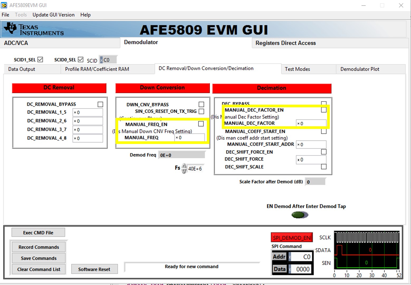
3. How to setup decimation factor to 32 to get sampling of 1.25MHz?

Thanks!

  • Hi Raunaq,

    We have received your query on the AFE5809. We'll get back to you on this within a week.

    Sincerely,
    Olu
  • Hi Raunaq,

    When you say that the previosuly applied voltage did not yield any results, what do you mean exactly? According to Page 32 of the datasheet, the linear range of the LNA is 1Vpk-pk. Anything exceeding that can lead to a distorted output signal.

    Furthermore, Page 65 of the datasheet shows how the register values affect the demod/down-conversion settings for the device.

    Sincerely,
    Olu
  • Hello,

    We are using 300mV pk-pk for input signal amplitude. In the datasheet, 250mV is minimum for LNA input. We are not reconstruct the external signal applied. When internal test pattern is applied, for example RAMP, it is reconstructed clearly. 

    Is there any particular setting we are missing for external signal?

    Thanks!

  • Hi Raunaq,

    Try out the different test modes and also verify that the DEMOD is setup for MSB first just like the ADC.

    Sincerely,
    Olu