Tool/software: Code Composer Studio
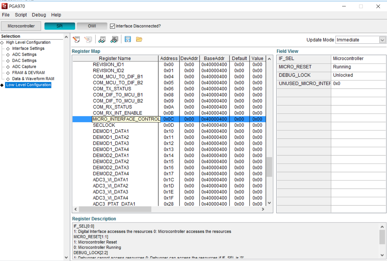
Can anybody give me an example SPI message that I could send to write a change to the MICRO_INTERFACE_CONTROL register in the PGA970, then read back the value of that register? As I understand SPI, I need to send a message that is:
{COMMAND} {ADDRESS} {DATA}
But I dont know what the command for read OR write is for the PGA970 and I'm not sure what the address map below means? Do I send the base address followed by the address followed by the DevAddr? So the command would be 0x???? 4000 0400 0C00 0001, where ???? is the write command that I want to know, 4000 0400 is what I believe the base address is from below, and 0C00 is the specific address following the BaseAddr, and 0001 is the data I want to write. Or maybe I've misunderstood SPI communications entirely? I'm fairly new to this...