This thread has been locked.

If you have a related question, please click the "Ask a related question" button in the top right corner. The newly created question will be automatically linked to this question.

PGA460: Problem in the connection of Small Form Factor Board with BOOSTXL-PGA460

Part Number: PGA460
Other Parts Discussed in Thread: , MSP-EXP430F5529LP, , DRV8870, DRV8816

Hello,

I would like to know what is the best method to connect the board PGA460Q1SFF-DDFB (460SFB Rev.E1) to the board BOOSTXL-PGA460.

Because i tried this method: On BOOSTXL-PGA460 EVB i did:

1) Elevate pins 10, 11 and 8 of PGA460

2) solder connectors on TP1, TP2, TP4

I connected the relative signals and I powered up the boards.

First issue was UV on VPWR, using just USB cable (VPWR went down to 5.1V, with a current consumption to the PGA460Q1SFF-DDFB of 15mA).

I solved this issue changing the PWR config, using external power supply (@7V)

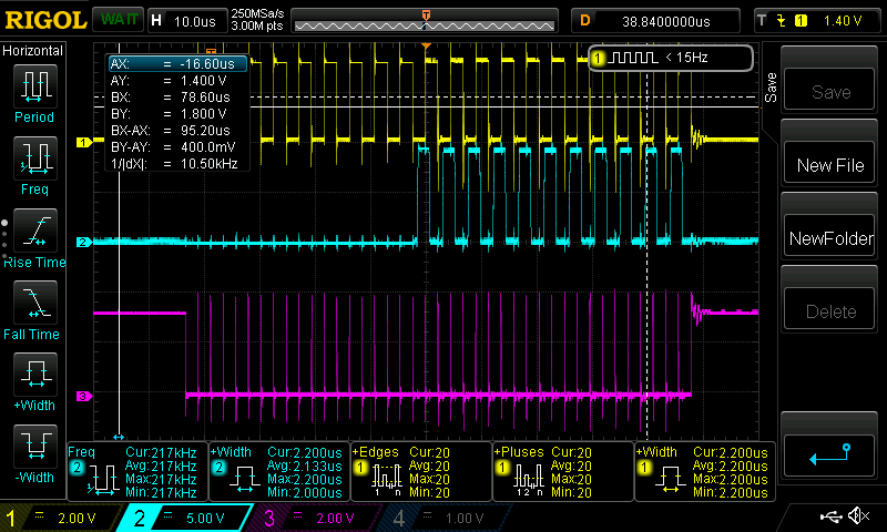
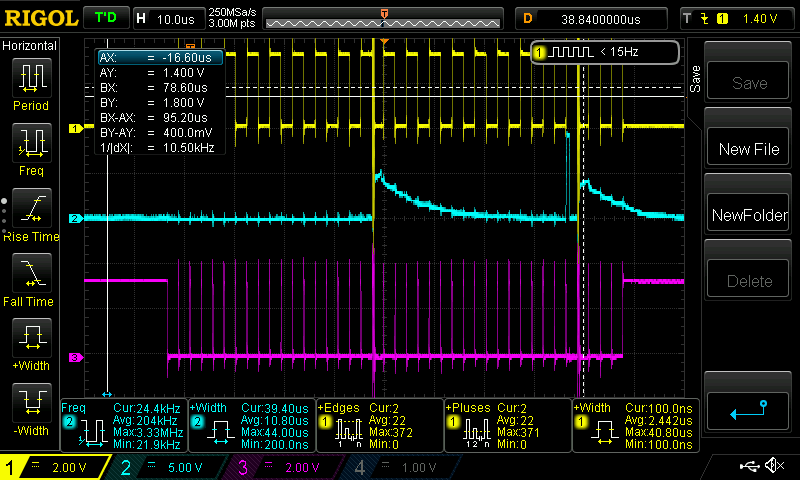
Now it is possible to configure the PGA460 on PGA460Q1SFF-DDFB (with a presaved config file), but when I try to make a measurement, the system is not working.

And i see this strange waveform on TXD line...attached you can find the picture...

I would like to know if it is correct or not...

Thank you for the support. Kind regards

Alessandro

  • Hi Alessandro,

    The USB boost supply on-board the BOOSTXL-PGA460 EVM can only supply enough power for a single PGA460 IC, so you are correct in that you need an external supply to power the DDFB module.

    To connect the PGA460Q1SFF-DDFB to the BOOSTXL-PGA460, you do not need to elevate any IC pins. You don't need the BOOSTXL-PGA460 if you only care about controlling the DDFB. You only need the MSP-EXP430F5529LP.
    Regardless, if you are controlling only the DDFB or not, make the following connections:
    •DDFB's J1-p3 (RXD) to BOOSTXL's J1-p4 (TXD_LP)
    •DDFB's J1-p4 (TXD) to BOOSTXL's J1-p3 (RXD_LP)
    •DDFB's J1-p1 (VPWR) to external supply
    •DDFB's J1-p2 (GND) to ground

    Then refer to PGA460 Frequently Asked Questions (FAQ) and EVM Troubleshooting Guide (www.ti.com/.../slaa733):
    5.5 Can I evaluate multiple PGA460 devices using the same UART bus of the PGA460-Q1 EVM?
    Yes, the GUI can be set to communicate with any PGA460 UART address, with a default UART address
    of 0 out of 7. To communicate to a non-0 UART address, navigate to the Interface Mode page, and select
    the UART Interface Address from the dropdown menu of the Command Selection box. To program the
    UART address to the selected address, click the Program to Selected Addr button underneath the
    dropdown. This does not burn the address to the EEPROM memory, and only writes to update the
    shadow register containing the UART address. To burn the new address to EEPROM, navigate to the
    Test Mode page, and click the Program EEPROM button. This will ensure that the UART address of the
    configured PGA460 is the newly programmed value.
    If an external PGA460 is connected to the BOOSTXL-PGA460 BoosterPack UART terminal,
    communication to the PGA460 installed on the BOOSTXL-PGA460 can be disabled by navigating to the
    Edit tab of the window menu, and clicking the Disable BOOSTXL-PGA460 Communication option. This
    allows communication commands to still transmit from the MSP-EXP430F5529LP, but prevents the master
    issued commands from reaching the on-board PGA460. This ensures that the external PGA460 device is
    exclusively contacted to prevent data collision, assuming both the on-board and external PGA460 devices
    shared the same UART address.
    (actual document shows supporting figures)

    For your DDFB schematic, are you supplying VX with an independent 26-45V supply? The restive voltage divider in the schematic as-is will only accept a VX voltage of 26-45V. If you have bridged VPWR to VX via R10, then your external 7V will not be enough to trigger the DRV8870 to toggle. If you want to use a VX of 7V, then you will need to modify the restive divider values at R2+R4 and R5+R8 so that 7V is scaled down to a 3.3V logic high at the DRV8870's IN1/2 pins. I recommend a resistor divider pair of 33.2kOhm and 26kOhm for both pairs. This gives you enough margin to increase VX up to almost 9V.

    See the recently released PGA460 Full-Bridge Driver Solutions for Ultrasonic Transducers (www.ti.com/.../slaa780) for details on how to interpret the PGA460-DRV8870 schematic.

    After you make the aforementioned changes, let me know if you still see the PGA460 TXD line issue.
  • Hi Akeem,
    thanks for your quick answer! Yesterday I was playing whole day with the board and I solved the issue exactly as you mentioned, changing the resistor divider R2+R4 and R5+R8.
    At the moment I want to supply the PGA at 10V, so I selected on both sides 22kohm resistors.
    I see that the square waves coming our from OUTA and OUTB pins have rising slopes very slow.
    These signals are not like a square wave, but more similar to a saw-tooth wave.
    So I changed the values, reducing it to 2.2kohm on both sides.
    Now the behaviour is really good. Do you see drawbacks on this? (apart the power consumption)
    I will check also the datasheet more in detail to understand the reason of this behaviour.
    Thank you also for the confirmation that i can use TXD_LP and RXD_LP (I was worried about the interaction with the GUI and the mux present on the board). I will modify the circuit as you suggested.
    Thank you so much for your support.
    Kind regards

    Alessandro
  • Hi Akeem,
    I've already tried to do the change for serial connection that you mentioned (using TXD_LP and RXD_LP), but the GUI cannot detect the PGA460. Could be the mux (U4) the reason of the issue? maybe does it do other actions?
    Let me know, thank you...my goal is to have the simplest HW connected to your GUI.
    Because I need to set up a demo of the system working, and the GUI is essential for:
    1) program registers
    2) see real time results of measurements
    Thank you, kind regards

    Alessandro
  • Hi Alessandro,

    Reducing the value of the resistor divider will only impact continuous current consumption. If your power budget allows for 2.2kOhm resistors, then I would recommend these values as well to guarantee a more robust square wave driver at the output of the DRV8870. As long as the IN1/2 pins are not exposed to more than 4V (abs max), the DRV8870 device will not become damaged, though I would aim to keep the logic level at 3.3V.

    The BOOSTXL-PGA460's TS3L501ERUAR comm switch can be disabled and completely isolate the LP's UART pins for use with an external PGA460 device by using the GUI's "Edit -- > Disabled BOOSTXL-PGA460 Communication" button. This disconnects the LP's UART pins from the BOOSTXL-PGA460's on-board PGA460. In this state, the on-board PGA460's communication pins will be floating. My initial thought was that the comm switch was not disabled, and you had data collision since both devices default to UART_ADDR 0. However, if you have verified that the comm switch has been disabled, and the only your external PGA460 device is connected to the LP's UART pins, then there must be a hardware connection issue. I can only reiterate that you ensure your TXD and RXD connections are not reversed, and that you have a common ground connection between the DDFB board and the LaunchPad.
  • Hi Akeem,

    sorry for the delay in my answer but I was very busy in the previous days...anyway now I'm back to this topic.

    About the logic levels, I see that the only one problem is related to U6 (SN74AUP1T87DCKR), that accept 3.3V levels.

    U3 (DRV8870) and U2 (SN74LVC2G04DBVR) can accept also more voltage on their pins, without issues...Right?

    Anyway this parte of the circuit is working fines at the moment.

    I have issues related to the output of U6...attached you can find some waveforms.

    I assembled 2 boards: checking the waveforms, both has the same behaviour on U6 output;

    but one is working properly (figure below)

    and the second one no (figures below)

    zoomed waveforms


    To make the second board working, I had to put and RC low pass filter on the output of U6, before the gate of N-mosfet (Q1).

    Did you ever had issues related to this topic? I think it is better to eliminate the spikes in the drive signal for Q1. What do you think about it?

    Changing topic: Do you have a similar part number of DRV8870, with a sleep mode that can be controlled by an external uP? (ex. DRV8816, but this chip has no output fast enough to drive load as required...we need 220kHz).

    Let me know, thank you and kind regards

    Alessandro

  • Hi Alessandro,

    U6 (SN74AUP1T87DCKR) is limited to 3.3V levels, while U3 (DRV8870) and U2 (SN74LVC2G04DBVR) are limited to 5.0V levels.

    Thanks for the oscilloscope waveform captures. I haven't encountered the failing Q1 gate drive issue as you have shown, but I will try to replicate this error, and improve the overall driver implementation to eliminate CH3's periodic low-to-high transient during the burst duration. Ideally, Q1 should be active/ON throughout the entire burst duration.

    Similarly to the DRV8816, the DRV8870 is also specified to a maximum of 200kHz, so you are already be using this part out of spec at 220kHz. I am not familiar enough with the DRV family to know which parts have a user controlled sleep modes. I recommend you post that question to the DRV family's E2E forum.
  • Hi Akeem,

    thanks for your answer.

    Let me know if you will have updates from gate driving solutions.

    Meanwhile I will continue to work on the system and also check if TI has proper solution in integrated motor's drivers.

    Thank you, kind regards

    Alessandro

  • For others following this post:

    The discussion for PGA460 full-bridge DRV alternatives has been continued at: e2e.ti.com/.../2360847