I have some questions about the test pattern generation in Radar Studio
- TestPattern Gen Timing -> In the documentation it states that samples are output at the System Clock of 200 MHz. How does this relate to data clock / frame clock. Inside my fpga logic the frame clock is 9.375 MHz but I cannot determine how this is governed.
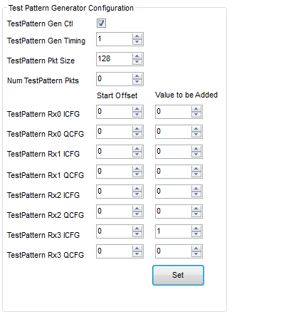
- TestPattern Pkt Size -> In the documentation it states that valid range is 64 - 1024 (4 RX complex), 64 - 2048 (4 RX real), 64 - 2048 (2 RX complex), and 64 - 4096 (2 Rx real). However in radar studio I cannot set a value greater then 255.
- Value Rollover -> I have included some graphics below. My first test had different starting and increment values but I could not make sense of what was coming across the line, so I simplified to have one channel I values increment and all the rest be zero. When I receive the data the RX3 I channel increments by 1 but it restarts back at 0 after reaching a count of 7.
- Random Values -> I have attached a chipscope plot data after shift register, and a hex editor view of data collected (hex editor data is packed RX0-3 I, RX0-3 Q). Again RX0-2 I/Q are all zeros but RX3 Q seems to be a random starting value and it random toggles to a different value.