


Other Parts Discussed in Thread: MSP430FR5969,
Hi,
I'm using two TDC7200s to measure the ToF in a LiDAR application. Up until this moment, I've been able to correctly set the SPI interface and correctly configure the registers.The start signal is given simultaneously to both by a PWM signal at 6.5kHz.
After the interrupt is detected in the TDC pin, the msp430 reads the data from both TDCs . The problem is when I read the measurement registers. Firstly, I've confirmed and I can successfully read the configuration registers and get the result of the initial setting. Furthermore, the registers TIME1 and CALIBRATION1 and CALIBRATION2 can also be read, giving a calibrated LSB value around 56ns. However, the problem comes when I read the CLOCK_COUNTER1 and I get 0x00. The CLOCK_CNTR_OVF is set to 0x10 (MSB byte to 0x00) to count up to 1us with a 16MHz external clock signal supplied by an MSP430FR5969, while the COARSE_CNTR_OVF is set by default to 0xFFFF. Before reading this value, I read the INT_STATUS register and obtained 0x1D, meaning that the CLOCK_COUNTER1 overflowed. Whatsoever, when I try to read the value in the register before starting a new measurement, I always obtain 0x00.
The implemented code is the following:
#include <msp430fr5969.h>
#include <SPI.h>


float f_p = 5, duty_cycle = 0.65;
float  ToF_1, ToF_2, calCount_1, calCount_2, normLSB_1, normLSB_2, range;
uint8_t restart[2] = {0b01000000, 0b10010011};
int restart_len = sizeof(restart)/sizeof(restart[0]);

uint8_t TIME1_1[3] = {}, CLOCK_COUNT_1_1[3] = {}, TIME2_1[3] = {}, CALIBRATION1_1[3] = {}, CALIBRATION2_1[3] = {};    // Buffers to load read values from TDC1
uint8_t TIME1_2[3] = {}, CLOCK_COUNT_1_2[3] = {}, TIME2_2[3] = {}, CALIBRATION1_2[3] = {}, CALIBRATION2_2[3] = {};    // Buffers to load read values from TDC1

void setup_PWM(float , float );
void setup_TDC();
void SPI_send(uint8_t *, int , int);
void SPI_receive(uint8_t *, uint8_t, int);
void ToF_read();

void setup() {                                                      // Setup the system
  PM5CTL0 &= ~LOCKLPM5;                                             // Disable the GPIO power-on default impedance mode

  Serial.begin(115200);

  P2DIR &= ~0x10;                                                   // Interrupt for TDCs
  P2REN |= 0x10;
  P2IES |= 0x10;
  P2IFG &= ~0x10;
  P2IE |= 0x10;

  P3DIR |= 0x10;                                                    // Output SMCLK
  P3SEL1 |= 0x10;


  setup_TDC();                                                      // Setup the TDCs
  delay(2);                                                         // Stabilize

  setup_PWM(f_p, duty_cycle);
}

void loop(){
  // ToF calculation
  calCount_1 = (int)(CALIBRATION2_1[0]*65536+CALIBRATION2_1[1]*256+CALIBRATION2_1[2])-(CALIBRATION1_1[0]*65536+CALIBRATION1_1[1]*256+CALIBRATION1_1[2]);  //2 Calibration periods
  normLSB_1 = (float)(62500/calCount_1);    // In picoseconds or else there is not enough resolution
  ToF_1 = (float)normLSB_1*0.001*(TIME1_1[0]*65536+TIME1_1[1]*256+TIME1_1[2]-TIME2_1[0]*65536-TIME2_1[1]*256-TIME2_1[2])+(CLOCK_COUNT_1_1[1]*256+CLOCK_COUNT_1_1[2])*62.5;

  calCount_2 = (float)(CALIBRATION2_2[0]*65536+CALIBRATION2_2[1]*256+CALIBRATION2_2[2])-(CALIBRATION1_2[0]*65536+CALIBRATION1_2[1]*256+CALIBRATION1_2[2]);  //2 Calibration periods
  normLSB_2 = (float)(62500/calCount_2);    // In picoseconds
  ToF_2 = (float)normLSB_2*0.001*(TIME1_2[0]*65536+TIME1_2[1]*256+TIME1_2[2]-TIME2_2[0]*65536-TIME2_2[1]*256-TIME2_2[2])+(CLOCK_COUNT_1_2[1]*256+CLOCK_COUNT_1_2[2])*62.5;

  range = (ToF_2 - ToF_1)*0.15;                                     // range in meters (divided by 2 to account forth and back)
  if(range>100) range = 100;                                        // Limiting the system. In practice it won't even be near this range value
  Serial.println(ToF_1);                                            // Send distance via UART to PC
  Serial.println(ToF_2);
  Serial.println(range);

  Serial.println(STATUS[0]);
}

#pragma vector=PORT2_VECTOR
__interrupt void PORT2_ISR_HOOK(void){
  for(int i=0;i<8;i++) nop;                                         // Guarantee both TDCs activate Interrupt
  ToF_read();                                                       // Receive data
  P2IFG &= ~0x10;
  P2IE |= 0x10;                                                     // Re-enable Interrupt
}

void setup_PWM(float f_pwm, float dc_pwm) {
  P1DIR |= 0x04;                                                    // P1.2 as the PWM output (dedicated pin)
  P1OUT &= ~0x04;
  P1SEL0 |= 0x04;

  TA1CTL |= TASSEL_2 | ID__1 | MC_1 | TACLR;
  TA1CCTL1 = OUTMOD_7;
  int T_0 = int(16000 / f_pwm);
  int T_1 = int(dc_pwm * T_0);
  TA1CCR0 = T_0;
  TA1CCR1 = T_1;
}

void SPI_send(uint8_t *data, int len, int sel) {
  (sel==1 ? P4OUT &= ~0x08 : (sel==2 ? P3OUT &= ~0x01 : P1OUT &= ~0x10));
  while (len){
    while(!(UCB0IFG & UCTXIFG));
    UCB0TXBUF = *(data++);
    while(!(UCB0IFG & UCTXIFG));
    UCB0TXBUF = *(data++);
    while (UCB0STAT & UCBUSY);
    len-=2;
  }
   (sel==1 ? P4OUT |= 0x08 : (sel==2 ? P3OUT |= 0x01 : P1OUT |= 0x10));
}

void setup_TDC(){                                                   // Configure both TDCs
  P3DIR |= 0x01;
  P3OUT |= 0x01;
  P1DIR |= 0x10;
  P1OUT |= 0x10;
  UCB0CTLW0 = UCSWRST | UCSSEL_2;
  UCB0CTLW0 |= UCCKPH | UCMSB | UCSYNC | UCMST;
  UCB0CTLW0 &= ~UCCKPL;
  P1DIR &= ~0b10000000;
  P1DIR |= 0b01000000;
  P1SEL1 |= 0b11000000;
  P1SEL0 &= ~0b11000000;
  P2DIR |= 0b00000100;
  P2SEL1 |= 0b0000100;
  P2SEL0 &= ~0b00000100;
  UCB0BR0 = 1;
  UCB0BR1 = 0;
  UCB0CTLW0 &= ~UCSWRST;

  uint8_t CONFIG1[] = {0b01000000, 0b10010011};
  uint8_t CONFIG2[] = {0b01000001, 0b00000000};
  uint8_t INT_MASK[] = {0b01000011, 0b00000101};
  uint8_t CLOCK_CNTR_OVF_H[] = {0b01000110, 0b0000000};
  uint8_t CLOCK_CNTR_OVF_L_1[] = {0b01000111, 0b00010000};
  uint8_t CLOCK_CNTR_OVF_L_2[] = {0b01000111, 0b00100000};

  int config_len = sizeof(CONFIG1)/sizeof(CONFIG1[0]);

  SPI_send(CONFIG1,config_len,2);
  SPI_send(CONFIG1,config_len,3);
  SPI_send(CONFIG2,config_len,2);
  SPI_send(CONFIG2,config_len,3);
  SPI_send(INT_MASK,config_len,2);
  SPI_send(INT_MASK,config_len,3);
  SPI_send(CLOCK_CNTR_OVF_H,config_len,2);
  SPI_send(CLOCK_CNTR_OVF_H,config_len,3);
  SPI_send(CLOCK_CNTR_OVF_L_1,config_len,2);
  SPI_send(CLOCK_CNTR_OVF_L_2,config_len,3);
}

void ToF_read(){                                                    // Read data from TDC whenever an interrupt is detected in P2.4
  // Receive data for TDC1 and TDC2
  SPI_receive(TIME1_1,0x10,2);
  SPI_receive(TIME1_2,0x10,3);
  SPI_receive(CLOCK_COUNT_1_1,0x11,2);
  SPI_receive(CLOCK_COUNT_1_2,0x11,3);
  SPI_receive(TIME2_1,0x12,2);
  SPI_receive(TIME2_2,0x12,3);
  SPI_receive(CALIBRATION1_1,0x1B,2);
  SPI_receive(CALIBRATION1_2,0x1B,3);
  SPI_receive(CALIBRATION2_1,0x1C,2);
  SPI_receive(CALIBRATION2_2,0x1C,3);

  // Restart measurement
  SPI_send(restart,restart_len,2);
  SPI_send(restart,restart_len,3);
}

void SPI_receive(uint8_t *buffer, uint8_t addr, int sel){
  (sel==2 ? P3OUT &= ~0x01 : P1OUT &= ~0x10);
  while(!(UCB0IFG & UCTXIFG));
  UCB0TXBUF = addr;
  for(int w=0;w<3;w++){
    while(!(UCB0IFG & UCTXIFG));
    UCB0TXBUF = 0x00;
    while (UCB0STAT & UCBUSY);
    buffer[w] = UCB0RXBUF;
  }
  while (UCB0STAT & UCBUSY);
  (sel==2 ? P3OUT |= 0x01 : P1OUT |= 0x10);
}
I've noticed another thing that may help. When I try the measurement in MODE 2, the register TIME1 does measure some values and I can read values other than 0. However, if I choose mode 1 I still can obtain a interrupt for COARSE_CNTR_OVF on INT_STATUS but when I read TIME1 I can only obtain 0x00 every time.
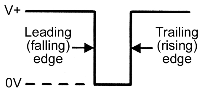
Another question, the input STOP pulse I'm having has a shape like below and I'm setting the STOP on the falling edge. Is there any problem ? Or the TDC automatically assumes a STOP if the STOP is kept at a high level?
Can anyone help?
Thanks in advance,
Joaquim
