This thread has been locked.

If you have a related question, please click the "Ask a related question" button in the top right corner. The newly created question will be automatically linked to this question.

IWR6843ISK: Power supply questions for the new mmWave radar ICs

Part Number: IWR6843ISK
Other Parts Discussed in Thread: IWR6843, , IWR1443, MMWAVEICBOOST

I'm currently working on developing a radar around the TI mmWave device family (looking specifically at the IWR6843) and have a couple questions on how the power is supplied in the development kit schematic (IWR6843ISK).

1) The RF supply of the IC could be connected directly to the main PMIC's (U4) 1.24V output since it's within the acceptable range, but an additional LDO (U5) is present to drop down to 1V. I understand that either 1.3V or 1V can be supplied to the IC, and it seems that the bypass resistor, R3, around the LDO allows for either option to be used.

Is the extra LDO used since it provides lower noise and/or better high-frequency performance than the main PMIC? Is it recommended to use such an LDO in both cases (i.e. 1.3V or 1V operation)?

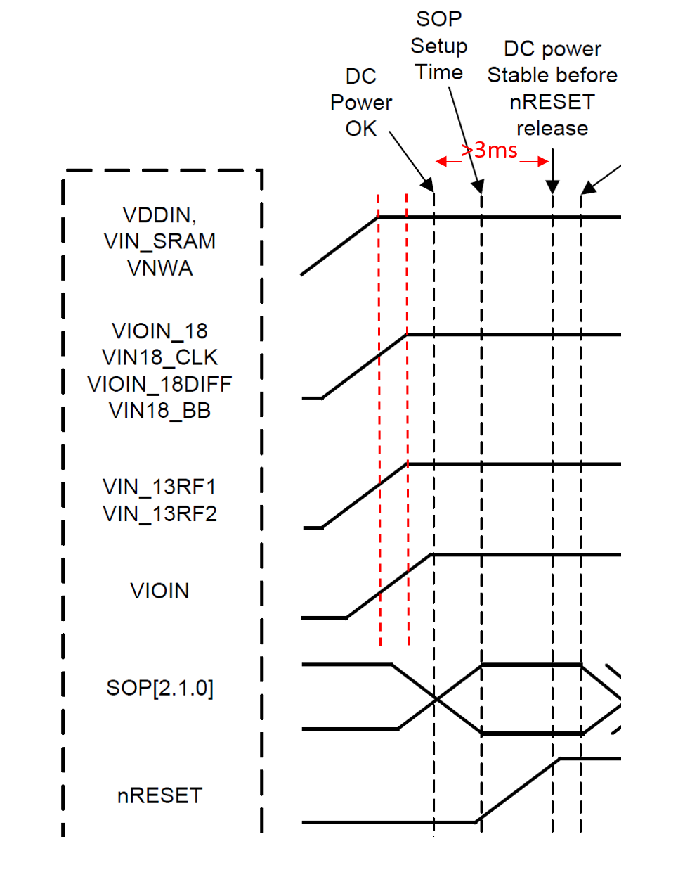
2) There's a load switch (U9) on the 3.3V (or 1.8V) supply to delay it's application to the IC. Again there's a resistor present to bypass it if desired. Under what conditions is this delay necessary, and is there any documentation available on power-up sequencing?

  • Ryan Sarver said:
    Is the extra LDO used since it provides lower noise and/or better high-frequency performance than the main PMIC? Is it recommended to use such an LDO in both cases (i.e. 1.3V or 1V operation)?

    If you enable LDO bypass in the firmware for the  IWR6843, you can supply 1V directly to the device, if the LDO bypass is disabled you need to supply 1.24V to the device. The 1.24V rails powers key RF blocks and voltage supplied to the rail affect RF performance.

    Ryan Sarver said:
    Under what conditions is this delay necessary, and is there any documentation available on power-up sequencing?

    Section 5.10.1 of the datasheet contains the  Power Supply Sequencing and Reset Timing information

    Regards,

    Charles O

  • Hi Charles,

    Thanks for your response.

    In the timing diagram that you mention it does look like there's a small delay on VIOIN (which would match the load switch on the schematic being on that supply) but unless I'm missing it I don't see what that delay corresponds to? The 'DC Power OK' dashed line doesn't match up with any other signals, so it seems to just indicate that all of the supplies are good.

    best,

    Ryan

  • Also, regarding your statement that 'voltage supplied to the rail affect RF performance', is there any kind of rule of thumb or quantitative way of analyzing that? For example, in the LP87524 datasheet, in Table 1 of Section 7.1, it specifies various configurations where the RF supply can either be powered directly or with an external LDO. I understand that the better the supply, the better the RF performance, but is there any way to determine what is 'good enough'?
  • Hi Charles,

    Just wanted to follow-up on this, not sure if you had the chance to see my responses?

    I'm trying to finalize my design and at the moment I haven't incorporated any kind of delay on VIOIN since I can't find any information on what it should be or why.

    Regarding the RF supply, I've decided to use the higher spec LDO (the TPS7A5301QRGRRQ1 as is used on the ISK) to have the best possible performance for this initial prototype.

    regards,
    Ryan
  • I've found this other thread here, which is about the IWR1443 but it seems it's more or less the same sequence as the IWR6843 from looking at the timing diagram: e2e.ti.com/.../720855

    The answer says that the reset pin shouldn't be asserted until at least 3ms after all four power rails have been established. I can't actually find that 3ms anywhere in either the 1443 or 6843 datasheet, but assuming a linear horizontal scale on the timing diagram (Figure 5-1 in the IWR6843 datasheet), it would seem to make sense in relation to the length of the 8ms shown for the MSS boot start.

    I was thinking of just adding a capacitor to GND on the nRESET pin to form a simple RC delay with the pull-up that's already there, ensuring at least 3ms before passing the input-high threshold of 1.57V on that pin.

    I'm still confused, however, by the design of the IWR6843ISK + MMWAVEICBOOST carrier. Looking at the schematics, there's the load switch, as I had previously mentioned, on the 3V3 (VIOIN) of the ISK, presumably delaying it to be applied about 100uS after the 1V8 supply. So I still don't understand why that's there, or if it's necessary.
    And secondly, it seems that the 3ms delay on the reset pin wouldn't be respected, as there's a 10k pull-up is on the MMWAVEICBOOST board with a 100nF cap to ground, providing only 646us delay before passing the 1.57V threshold (if my calculations are correct).

    I'm trying to finalize my design and I currently don't have that load switch on there, so I just want to make sure I'm not going to be in for any nasty surprises finding out that actually VIOIN has to be applied after the 1V8.

  • Hi,

    If you follow the timing diagram in the datasheet. basically ensuring that the lines get to steady state in the right sequence you should be fine.

    Regards,
    Charles O
  • Hi Charles,

    I'm sorry but this isn't answering my question. I understand that some kind of timing sequence needs to be respected, but it's not at all clear from the image in the datasheet what that timing sequence is.

    In the hardware checklist I saw mention of the 3ms delay after the lines are stable before asserting the reset, so I'm following that.

    But I'm worried by the fact that the datasheet picture appears to show the VDDIN supply activating first, followed by the VIOIN_18 and VIN13RFx supplies at the same time, and finally the VIOIN (see photo below, where I drew in extra lines in red to make my question more clear:

  • Hi,

    As shown in the snippet you attached, please make sure the lines activated in the same sequence and the steady state is reached in the same sequence shown. I hope this answers the question

    Regards,
    Charles O
  • But there are no specified minimum delays?
  • Yes. The time for the voltage rails to settle will vary from PMIC to PMIC so specifying the delay is not a feasible option

  • I find it strange that a certain power-up sequence is required, but no information (even ballpark) can be given on what the delays between the rails being applied should be.
    1ns? 1ms? 100ms?
    Even the IWR6843ISK doesn't seem to respect this sequence, with VDDIN, VIOIN_18 and VIN_RF all being applied at the same time, and only VIOIN being delayed by the load switch.
    I'm going to just use that same configuration on my design then, but it's a shame that I don't understand the actual requirement.
  • Hi,

    We will make amendments and add more details to the datasheet as needed .
    However as indicated earlier there are factors including the PMIC used that can vary the timing of the various voltage rails.

    Regards,
    Charles O