This thread has been locked.

If you have a related question, please click the "Ask a related question" button in the top right corner. The newly created question will be automatically linked to this question.

AWR1642: Demo-board questions

Part Number: AWR1642

Team, 

Please help answer these AWR1642 EVM related questions:

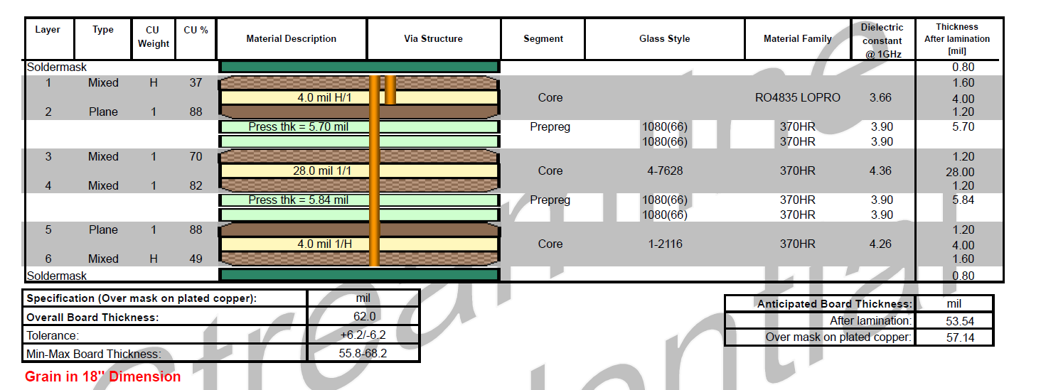
  1. For the AWR1642 demo-board:
  1. What’s the PCB substrate material?
  2. What’s the dielectric constant of the substrate?
  3. What’s the laminate thickness? i.e. too thick laminate thickness can resonate and even propagate its own waves.


  1. Patch antenna:
  1. What’s the planar patch antenna etch material?
  2. What’s the Transmission line characteristics? e.g. microstrip, strip or co-planar waveguide?
  3. What’s the antenna array geometries: Microstrip inset fed structures, coaxial cable fed and aperture coupled.
  4. What’s the antenna Field of view (Beam width) of the AWR1642 gesture radar?
  5. What’s the Beam forming technique used (e.g. Butler Matrix or Rotman Lens?)


  1. Does TI have a recommended PCB manufacturing house?

 Thanks

Viktorija

  • Hello Viktorija,

    Regarding the first three questions, you can refer to the below stack up.

    I will get back to you with answers to the remaining questions.

    Regards,

    Adrian

  • Hello Viktorija,

    Regarding the patch antenna questions:

    1. Can you clarify what you mean by etch material? The antenna material is copper with an immersion silver finish. The etch process we recommend is laser direct imaging etch mask for tighter tolerances.

    2. The EVM uses a grounded coplanar waveguide.

    3. The EVM antenna uses a microstrip feed line transitioned into the GCPW.

    4. The FOV of the AWR1642BOOST is 120 degrees azimuth. The FOV of the AWR1642BOOST-ODS is 160 degrees azimuth.

    5. The AWR1642 does not support beam forming.

    Regards,

    Adrian
  • Thanks a lot for the feedbacks. I'll review and respond shortly.

    Thanks,

    John